
Electronicseng EmbeddedSystems: Bluetooth Modular Keyboard Notes with Keybit, Keyword, I2C Pogo Pins, and 1u PCBs
This EmbeddedSystems review on Electronicseng focuses on the engineering structure behind Keybytes: a keyboard in which each key is a separate 1u PCB, called a Keybit. The central design questions are module identity, bus wiring, programming access, power conversion, and mechanical mounting. The base controller, called the Keyword, adds Bluetooth and USB, while the individual key modules each depend on a CH32V003 RISC-V device. The text below keeps the published facts as the boundary and reorganizes them for embedded bring-up, debugging, and design comparison.
Video and visual evidence
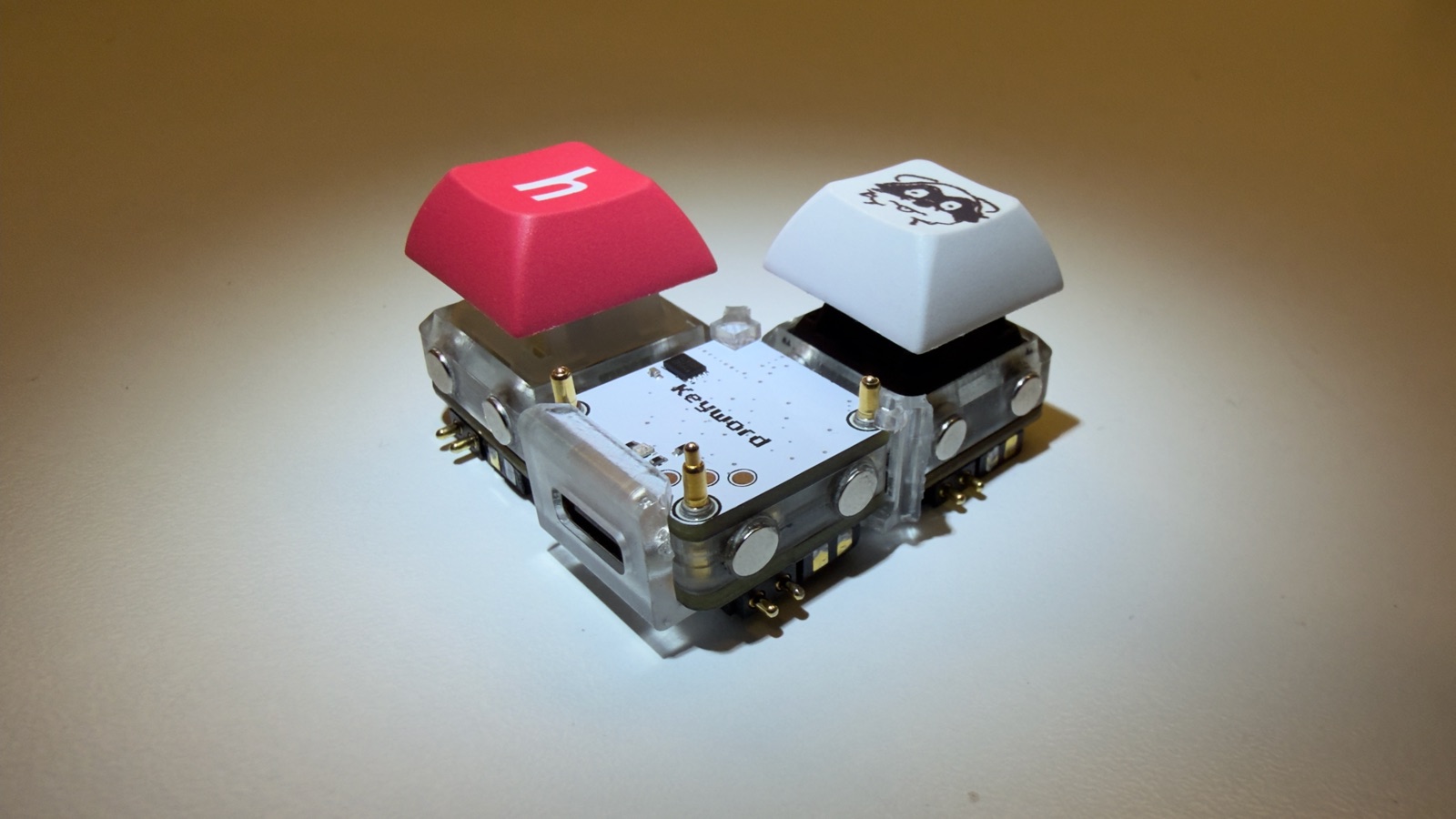
keybytes-demo.mp4
The supplied visual material covers the assembled modular keyboard, the demo clip, the Keybit schematic, the Keybit layout, the Keyword layout, two Keyword 3D views, and the finished keyboard with magnetic cases. These views can be checked against the text to confirm the board-level partitioning before tracing signals.
Architecture at a glance
- The layout is rearrangeable because every key is its own 1u PCB, the Keybit.
- Each Keybit centers on a Cherry MX switch and a CH32V003 RISC-V microcontroller.
- The Keyword main board adds Bluetooth and USB through an STM32WB55RGV6.
- Pogo pins on all 4 sides of every Keybit carry 3.3V, GND, and I2C to the Keyword or to other Keybits.
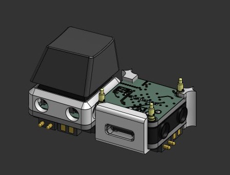
- Magnetic cases hold the modules together.
- Key programming is performed from the main board over the pogo pins; the Keybit also exposes corner pads for programming.
- A 2MB QSPI flash part, the W25Q16JV, stores the key firmware.
- Battery charging uses a BQ25895 and includes solder pads for a 1S LiPo.
- A TPS631000 buck-boost converter is included on the Keyword.
- Board state can be indicated by an RGB status LED.
- Power enters through USB-C with ESD protection.
- A ceramic Bluetooth antenna is used for the wireless path.
Comparison table: Keybit module and Keyword controller
| Design aspect | Keybit | Keyword |
|---|---|---|
| Board size | 1u; 19.05mm x 19.05mm | Both boards are 1u; the Keyword is split into two stacked PCBs |
| Core device | CH32V003 RISC-V microcontroller | STM32WB55RGV6 |
| Human interface role | One key, one Cherry MX switch | Main board that connects Keybits and provides USB and Bluetooth |
| External connection | Pogo pins on all 4 sides carry 3.3V, GND, and I2C | Stacked upper and lower PCBs; upper carries STM32WB55RGV6, antenna, and flash; lower carries USB-C, charger, and converter |
| Firmware or data storage | Can be programmed through corner pads and from the Keyword | 2MB QSPI flash (W25Q16JV) stores key firmware |
| Programming interface | Corner pads are present for programming | 3 pogo pins on the top are used to program the Keybits |
| Power features | Receives 3.3V through the shared pogo-pin path | BQ25895 for a 1S LiPo, TPS631000 buck-boost, USB-C with ESD protection, RGB status LED |
Step-oriented bring-up notes
- Start from the KiCad designs and identify the two boards, Keybit and Keyword; both are 1u (19.05mm x 19.05mm).
- Trace the Keybit first: confirm the Cherry MX switch, the CH32V003 RISC-V device, the four-sided pogo pin pattern, and the corner programming pads.
- Verify the module bus: the pogo pins on all 4 sides are intended to carry 3.3V, GND, and I2C between the Keyword and other Keybits.
- Move to the Keyword: separate the stacked two-board concept. The upper side includes the STM32WB55RGV6, the ceramic Bluetooth antenna, and the W25Q16JV flash; the lower side includes USB-C, the BQ25895 charging circuit, and the TPS631000 buck-boost converter.
- For programming access, note that the top side of the Keyword exposes 3 pogo pins, while the Keybit also has corner pads. Programming is performed from the main board over the pogo pins.
- Before attaching the magnetic cases, check the RGB status LED, the 2MB QSPI flash role, and the 1S LiPo solder pads against the layout.
Common misconceptions
- The design is not described as a fixed single-PCB keyboard matrix; every key is its own 1u PCB.
- The Keyword is not one board; it is split into two PCBs that stack on top of each other.
- The Keybit pogo-pin interface is not a purely mechanical contact; the published signals are 3.3V, GND, and I2C on all 4 sides.
- The programming detail is not limited to one pad type: the source lists corner pads on the Keybit and 3 pogo pins on the Keyword.
- The wireless function is not only an antenna item; the board uses an STM32WB55RGV6 with a ceramic Bluetooth antenna.
Keybit details
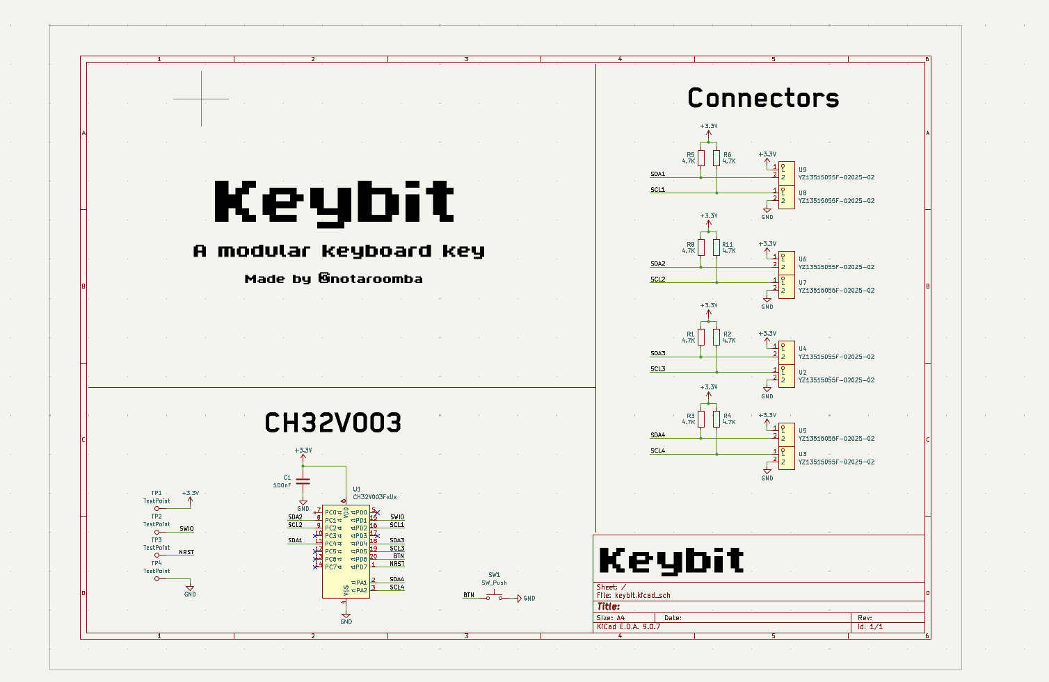
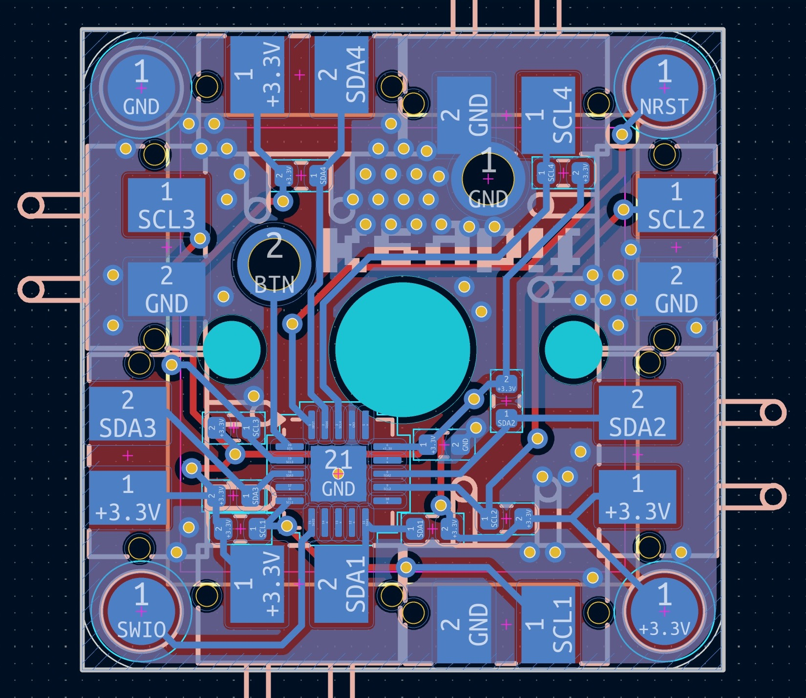
The Keybit is the single-key PCB. It uses a Cherry MX switch and a CH32V003 RISC-V microcontroller. Pogo pins on every side carry 3.3V, GND, and I2C, so the module can connect to the Keyword or to another Keybit. Corner pads are provided for programming.
Keybit schematic:
Keybit layout:
Keyword details
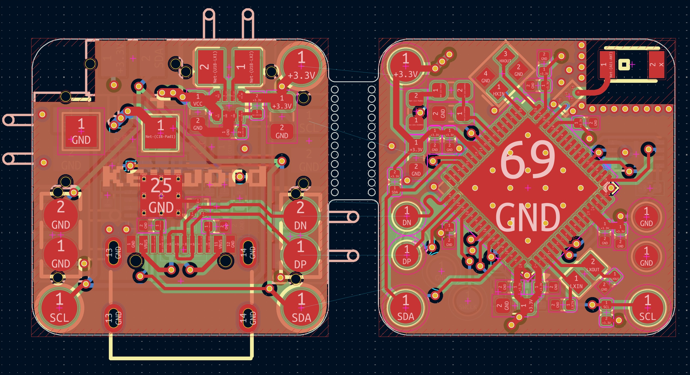
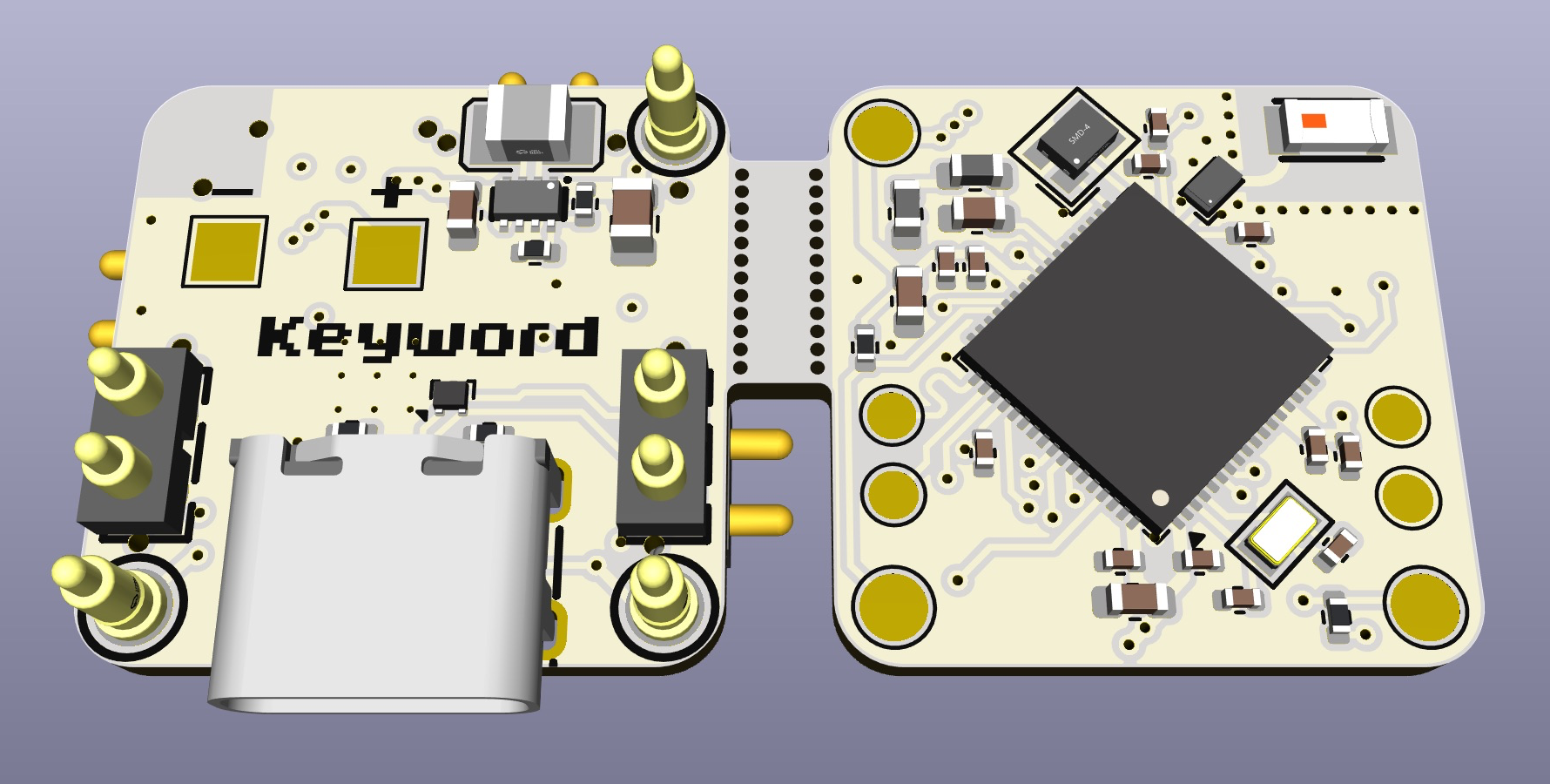
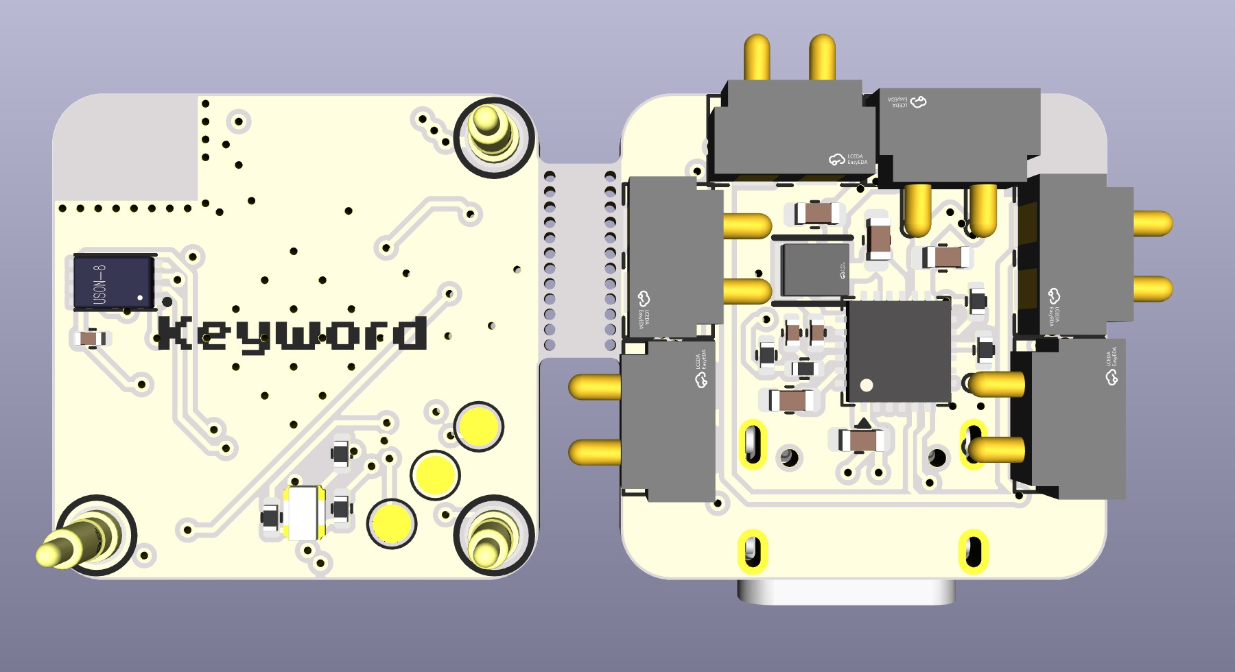
The Keyword is the main board to which Keybits attach. The implementation is split into two stacked PCBs. The upper board carries the STM32WB55RGV6, the ceramic Bluetooth antenna, and the W25Q16JV flash. The lower board carries USB-C, the BQ25895 charger for the 1S LiPo solder pads, and the TPS631000 buck-boost converter. The top side exposes 3 pogo pins for Keybit programming.
Keyword layout:
Keyword 3D view from the top angle:
Keyword 3D view from the bottom side:
Case and mechanical mounting
The cases are custom-designed in Onshape, and the STEP files are provided in the cad folder. The magnetic cases hold the modules together.
Toolchain, credits, and project references
The published project credits KiCad, Onshape for case design, Blender for 3D renders, STM32CubeMX, and Hack Club Forge. Related project references in the source material are Ember, Cyberboard, Trace, and Linea.
- Ember, a USB-C powered reflow hotplate with Bluetooth.
- Cyberboard, a development board sized to match a Raspberry Pi Pico and based on STM32 with Bluetooth.
- Trace, a PCB ruler that includes reference footprints.
- Linea, an EMR tablet.
FAQ for EmbeddedSystems readers
Why is the keyboard reconfigurable?
Because the layout can be rearranged: every key is its own 1u Keybit PCB rather than part of a single fixed layout.
What controller sits inside each key?
Each Keybit uses a CH32V003 RISC-V microcontroller.
Where do Bluetooth and USB come from?
The Keyword main board provides Bluetooth and USB through the STM32WB55RGV6.
How are neighboring modules connected?
Pogo pins on all 4 sides of each Keybit carry 3.3V, GND, and I2C.
How are Keybits programmed?
Programming is performed from the Keyword over the pogo pins. The Keyword top exposes 3 pogo pins for this purpose, and the Keybit corner pads are also used for programming.
What stores the key firmware?
A 2MB QSPI flash, the W25Q16JV, stores the key firmware.
What power path and indicators are present?
USB-C with ESD protection feeds the lower Keyword board. Battery charging uses the BQ25895, including solder pads for a 1S LiPo. The TPS631000 buck-boost converter is included, and an RGB status LED is present.
What license applies?
The published license is MIT.
Action checklist for embedded readers
- Read the text with the KiCad boards, Keybit schematic, Keybit layout, and Keyword layout open.
- Use the comparison table to separate the per-key CH32V003 role from the Keyword STM32WB55RGV6 role.
- Confirm the exact mechanical and electrical anchors: 1u, 19.05mm x 19.05mm, all 4 sides, 3.3V, GND, I2C, two stacked Keyword PCBs, 3 programming pogo pins, 2MB QSPI flash, BQ25895, 1S LiPo, TPS631000, USB-C, ESD protection, RGB status LED, and ceramic Bluetooth antenna.
- For case work, use the Onshape STEP files in the cad folder, because the published design uses magnetic cases to hold the modules together.
- When evaluating similar builds, keep Ember, Cyberboard, Trace, and Linea as reference points from the source material; they are not additional features of the keyboard itself.
This EmbeddedSystems note on Electronicseng summarizes the Keybit/Keyword design using the available project data and the MIT-licensed source material.