
One-Cycle Settling for PWM DAC Ripple: The Unicycle Filter Idea, Revisited for General Electronics Design
Ask an electronics engineer to turn a PWM output into an analog voltage and the first objection is rarely the duty cycle — it is the filter. The low-pass network needed to tame ripple is exactly what makes the output slow to reach a new value, and shortening that delay normally means letting more ripple through. The trade-off is usually presented as fixed. Two pieces of Design Ideas material, one current and one from the archive, frame the problem differently: synchronize the filter to the modulation cycle itself, and the settling question collapses to a single cycle.
What follows is a walk-through aimed at general engineering practice rather than at one component note — what was measured, how the numbers normalize, what must be true in hardware, and which of those assumptions transfer to unrelated analog tasks.
Where the question started
In the recent Design Idea “DAC implementations: The spread-bit PWM strikes back”, Christopher Paul compares spread-bit and clustered-bit PWM DAC results at length. The portion carrying the most transferable information is the detailed settling-time tabulation for spread-bit DACs in Table 1. Read alongside Christopher's precision 3 rd order unity-gain ripple filter design, those data describe peak-to-peak ripple amplitudes of Vpp = 1/N.
The useful move is normalization. Once the results are expressed against the PWM cycle length, 2 b / 1mHz clock, and common resolutions from 8 to 16 are tabulated, the number of PWM cycles needed for the output to settle within one LSB stops behaving the way a designer might expect: it hovers around only 2 to 3 cycles. That is an impressive result, and it raises the obvious follow-up — could the outcome be made a bit better?
The answer is an old one
Pursuing that follow-up leads into the Design Ideas archives from nearly two decades ago, specifically to the circuit in Figure 1 of “Fast-settling synchronous-PWM-DAC filter has almost no ripple”. That design does not fight the low-pass problem harder; it sidesteps much of the difficulty. Its architecture is a differential integrator, A1, and a sample-and-hold amplifier, A2, arranged in a feedback loop synchronized with the PWM cycle — T2 in the timing figure of the original article.
What makes one cycle possible
Two relationships define the behavior:
- Time constant equal to the PWM period: with the integrator time constant set to R1C1 = T2, the integrator spans exactly one cycle.
- Capacitance equality: with the sample capacitor C2 equal to the hold capacitor C3, acquisition and hold share the same charge accounting.
Together they let the filter acquire and settle to a new DAC value in exactly one PWM-cycle time — the “unicycle!” outcome. Ripple rejection of the synchronous filter is theoretically infinite, which is what puts it in a different category from the ordinary accumulation of PWM cycles. In practice the ceiling is the switch, not the theory: the limiting factor is nonzero charge injection from S2 into C3. Choosing a low-injected-charge switch for S2 and generous capacitances for C2 and C3 brings ripple amplitudes onto the order of microvolts.
For a general audience the pattern is worth naming explicitly. When a rejection figure is unlimited on paper, the real design task becomes identifying the single non-ideal mechanism that survives the theory — here, injected charge — and sizing around it.
Bringing the legacy circuit up to date
Figure 1 below shows that archived topology refreshed with an integrator time-constant settling-time trim, R1.
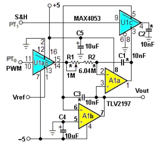
Figure 1 This “unicycle” DAC ripple filter combines a differential integrator, A1a, with a sample-and-hold amplifier, A1b, in a feedback loop operating synchronously with the PWM and sample-and-hold timing signals. Note that the integrator time constant shown is centered around 65.4ms and 16bit “clustered bit” PWM resolution.
R1 is adjusted until the single-PWM-cycle unicycle settling is exact. That one adjustment effectively compensates for and cancels the C2 and C3 tolerance, absorbs the tolerances of the remaining integrator feedback-loop passives — R2, C1, C2 and C3 — and even covers the U1 internal switch Rons. In other words, this simple modification removes the 2008 Design Idea requirement that single-cycle settling depend on C2 and C3 being precisely equal.
Accuracy is not what the trim touches
Neither R1 nor the passive component tolerances affect the conversion accuracy of Vout = PWMdutycycle x Vref; that accuracy is inherent. What remains are small effects caused by op amp A1 non-idealities, mainly finite DC gain and input offset, plus single-digit-ohms of U1 internal switch mismatch. The mismatch is reduced by paralleling the U1a and U1b sections shown in Figure 1.
The timing check
If R1 is adjusted so that (R1 + R2)C1C3/C2 = Tpwm = 2 16 /1MHz, a precise unicycle settling completes in exactly one 16-bit 65.536ms PWM cycle time, as shown in Figure 2. The final Vout = PWMdutycycle x Vref stays inherent and unaffected by the R1 adjustment or by passive part tolerances.
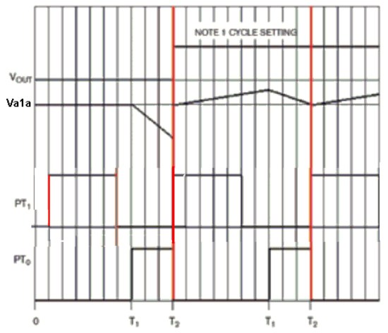
Figure 2 The settling timing sketch that details the unicycle result.
No firmware dependency
Worth separating out: this rapid settling does not rely on spread-bit techniques and their dependence on software execution times. Because a microcontroller's built-in PWM peripherals can generate the timing signals, order-of-magnitude faster PWM frequencies become available — and even faster settling times, if a design requires them.
A reusable setup checklist
- Normalize before comparing: convert settling figures into PWM cycle counts at 2 b / 1mHz clock, then review them across resolutions 8 to 16.
- Record the baseline: spread-bit data plus a 3 rd order unity-gain ripple filter give Vpp = 1/N and roughly 2 to 3 cycles.
- Set the integrator time constant to the PWM period, R1C1 = T2.
- Start from C2 equal to C3, then let one trim do the matching work.
- Adjust R1 until settling is exact within a single PWM-cycle time.
- Verify the closed form: (R1 + R2)C1C3/C2 = Tpwm = 2 16 /1MHz for the 16-bit 65.536ms case.
- Select a low-injected-charge device for S2 and generous values for C2 and C3 to keep ripple in the microvolt region.
- Parallel U1a and U1b to shrink the single-digit-ohms internal switch mismatch.
- Leave the duty-cycle-to-Vref relationship alone — accuracy there is inherent, not trimmed.
- Drive the timing from MCU PWM peripherals rather than software bit spreading when frequency matters.
Two ways of settling, side by side
| Aspect | Reference comparison | Synchronous “unicycle” filter |
|---|---|---|
| Source | Christopher Paul, Table 1 in “DAC implementations: The spread-bit PWM strikes back” | Legacy Design Idea, “Fast-settling synchronous-PWM-DAC filter has almost no ripple” |
| Cycles to settle, normalized | About 2 to 3 cycles across 8 to 16 | Exactly one PWM-cycle time |
| Ripple picture | Vpp = 1/N with the 3 rd order unity-gain filter | Theoretically infinite rejection; practical floor from S2 charge injection into C3, microvolt order after part selection |
| Matching burden | — | Originally C2 = C3; an R1 trim now covers R2, C1, C2, C3 and U1 switch Rons |
| Timing dependency | spread-bit methods tie results to software execution times | Runs from built-in microcontroller PWM peripherals |
| Bit organization | Both spread-bit and clustered-bit (“clustered bit”) cases compared | Settling independent of spread-bit technique |
Common misconceptions
“Settling is purely a filter-order problem”
The archived circuit answers by placing the integrator and the sample-and-hold in a loop synchronized to the PWM cycle, sidestepping much of the difficulty of low-pass filtering rather than adding more filter to it.
“Theoretical rejection makes the practical limit irrelevant”
The opposite matters. Infinite rejection is the paper result; the achievable figure is decided by charge injection from S2 into C3, which is exactly why switch choice and capacitance sizing appear in the design guidance.
“Precision-matched capacitors are mandatory”
They were in the 2008 version, where single-cycle settling depended on C2 and C3 being precisely equal. With the R1 settling-time trim, one adjustment cancels that tolerance along with the other feedback-loop passives.
“Trimming the time constant will shift the output value”
It does not. Vout = PWMdutycycle x Vref is inherent, and neither R1 nor passive tolerances move it; the residual errors come from A1's finite DC gain and input offset and from the U1 switch mismatch.
“Fast settling needs spread-bit firmware”
The result does not rely on spread-bit techniques or on software execution times, so the microcontroller's own PWM peripherals can supply the timing.
FAQ
What does “unicycle!” mean in this context?
It names a filter that acquires and settles to a new DAC value in exactly one PWM-cycle time instead of taking several cycles.
Where do the 2 to 3 cycle figures come from?
From the spread-bit settling tabulation in Table 1, after normalizing to the PWM cycle length, 2 b / 1mHz clock, and tabulating resolutions from 8 to 16.
How much ripple should a designer expect?
In the reference comparison, Vpp = 1/N when the data are combined with the precision 3 rd order unity-gain ripple filter. In the synchronous filter, rejection is theoretically infinite, with real ripple on the order of microvolts once a low-injected-charge S2 and generous C2 and C3 are chosen.
Which resolution and period do the updated figures assume?
A 16bit “clustered bit” case centered around 65.4ms in Figure 1, and one 16-bit 65.536ms PWM cycle in the Figure 2 timing sketch, derived from Tpwm = 2 16 /1MHz.
What still limits accuracy after everything is trimmed?
Small effects from op amp A1, mainly finite DC gain and input offset, plus single-digit-ohms of U1 internal switch mismatch, which paralleling U1a and U1b reduces.
Is any of this reusable outside PWM DACs?
The transferable part is the framing: match the integrating time constant to the modulation or sampling period, keep acquisition and hold elements consistent, and let one trim absorb component tolerances instead of specifying those tolerances away.
Closing notes
For general electronics work the lesson is less about PWM DACs than about where to look for headroom. A comparison already considered strong — 2 to 3 cycles, normalized — was improved not by adding filter stages but by synchronizing the filter to the cycle and trimming one resistor. The same posture carries across analog and mixed-signal tasks: quantify the baseline, normalize before judging, isolate the single mechanism that breaks the ideal case, and design around that one thing.
Prepared for Electronicseng by Rachel Williams. Original material credit: the legacy design comes from Stephen Woodward, whose relationship with EDN's Design Ideas column goes back to a first contribution in 1974; more than 200 submissions have been accepted, including best Design Idea of the year in 1974 and 2001.