
Crossing about 100 V and >1000 V with Voltage Multipliers: A Practical Electronicseng View
For Electronicseng readers, the point is to treat voltage multipliers as a general engineering method rather than a niche trick. A stack of diodes and capacitors can push a low input higher by two or three, or even hundreds, but the design conversation changes once output passes about 100 V and reaches >1000 V.
Many high-field systems need only modest current, commonly 100 mA or less, which makes capacitor-diode stacking attractive for X-ray equipment, physics experiments, beam steering, electric-field shaping, lightning simulation, and electrostatic tests. For this site, the practical takeaway is that the work shifts from power delivery to electric-stress management.
Why not start with a transformer?
A transformer could theoretically produce large step-up ratios, such as 10× or 1000×. The practical penalty appears as ratio and secondary voltage grow: core and copper losses reduce efficiency, while wire insulation confronts dielectric stress that may exceed its limits. Flyback converters are a real solution when energy storage and conversion are integrated, and one familiar case was the cathode-ray tube display that dominated consumer video for over 50 years before LED/LCD panels displaced it.
The rectifier stack idea
Passive voltage multipliers usually place capacitors and diodes in a ladder. Each stage reuses the previous stage charge, so the circuit becomes a specialized rectifier chain that can develop an integer multiple of the AC peak value, commonly ×2, ×3, or ×4, in the ideal case. A three-stage multiplier illustrates the sequence: each line cycle charges capacitors, and after several cycles the capacitors each approach the peak input voltage, then the series connection adds those voltages at the output.
Take a 120 VAC rms supply: its peak value is 170 V. The capacitors are not being boosted by mysterious switching; they are charged by rectification and then stacked. Diodes act as passive switches: they allow charge into the capacitors while blocking return discharge when the AC input falls. Reversing all diodes and capacitor polarities produces a negative output instead.
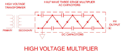
Figure 1. A capacitor-diode ladder stores AC peak charge stage by stage, then presents the series sum at the output. Image credit: Spellman High Voltage Electronics Corporation.
| Approach | Where it fits | Design watch-outs |
|---|---|---|
| Transformer or flyback | When a step-up path needs 10× or 1000×, isolation, or more continuous power transfer | Losses, insulation stress, magnetics construction |
| Passive multiplier | When ×2, ×3, or ×4 stacking from AC peaks is enough, especially near 100 mA or less | Stage voltage ratings, sag under load, cleanliness of layout |
| High-voltage layout discipline | When any circuit moves toward about 100 V and beyond | Sharp edges, corona, spacing, protection |
Selection limits before layout
Parts ratings are the first real wall. A component across a multiplier stage must tolerate at least twice the peak voltage seen there, so designers normally start from a 120 VAC line and a 170 V peak, then apply safety margin. If a 10× multiple is required, the calculation already points to at least 1700 V, and a derating factor such as ×2 or more should remain in the BOM review.
Load regulation is the second wall. The stored charge is finite; once the load takes current, voltage sags. This is tolerable for field generation and instrumentation, but it makes the topology unsuitable when the output must supply sustained power.
Material behavior is not linear
The high-voltage world has many transition points; designers often call the behavior strange because rules that work at low voltage stop working cleanly. A useful analogy is water passing through freezing or boiling: below or above each region, the rules feel simple, but crossing the boundary changes the failure mode. Corona discharge from sharp metal points is one example: it can pit contacts and destroy insulation.
Even small things such as solder geometry matter. A normally acceptable joint can leave edges and cold solder points that encourage ionization. That is why ball soldering is common in high-voltage assemblies: a larger, smooth spherical joint lowers local electric-field stress and reduces corona risk. Figure 2 shows the construction principle.
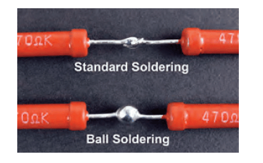
Figure 2. Physical construction is part of the electrical design: rounded joints reduce sharp points that can initiate discharge. Image credit: Maker Forums.
Safety is not an optional step
A multiplier schematic does not imply a safe build. This domain has hidden requirements beyond the drawing: spacing, insulation, material defects, component aging, and overvoltage protection all matter. Just being careful is not enough, because a tiny oversight can be lethal. Specialty fuses and protection devices are often required; if a design is intended for sale, regulatory obligations add further review. Someone may post a project reaching tens of kilovolts, but the correct response is not to copy it casually. For Electronicseng work, treat high voltage as a supervised activity: experienced personnel, clear emergency procedures, and verified discharge paths.
Applications that justify the topology
Some applications use multiplier output because the benefit comes from high electric field, not high continuous power. A team at MIT built a free-flying aircraft with a wingspan of a few meters and no moving parts in its propulsion system. The lift mechanism uses negative ions moving through the field generated near the wing rear edge, attracted to a 20-kV fence structure. The on-board subsystem receives 200 V DC from batteries and uses a 600-W power path designed by the Power Electronics Research Group in the MIT Research Laboratory of Electronics.

Figure 3. High voltage enables unusual applications such as the MIT ion-driven aircraft, where a 20-kV field structure at the trailing edge attracts ions. Image credit: MIT.
The architecture combines a switching regulator, a 1:15 step-up transformer, and a six-stage Cockcroft-Walton voltage multiplier to produce 20 kV DC. The same family appears in accelerator history under a slightly different spelling: Cockroft-Walton.
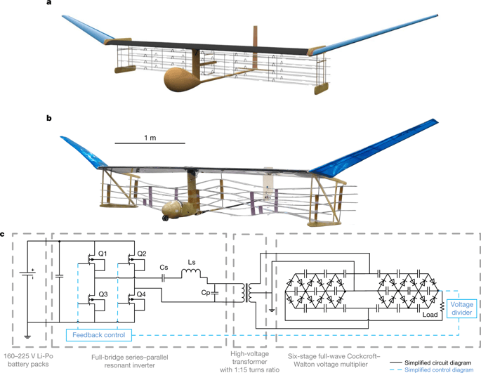
Figure 4. The MIT subsystem converts 200 V DC into a 20 kV DC output using a switching stage, a 1:15 transformer, and a six-stage Cockcroft-Walton multiplier. Image credit: MIT.
Cockroft-Walton generators have long served as injectors for particle accelerators. A 750-kV machine commissioned in 1975 at CERN is a reminder of scale: it produced up to 750 kV and is about 12 feet (~3 ½ meters) tall, not a desktop unit. Modern descriptions note that larger units can reach the single-digit megavolt range.
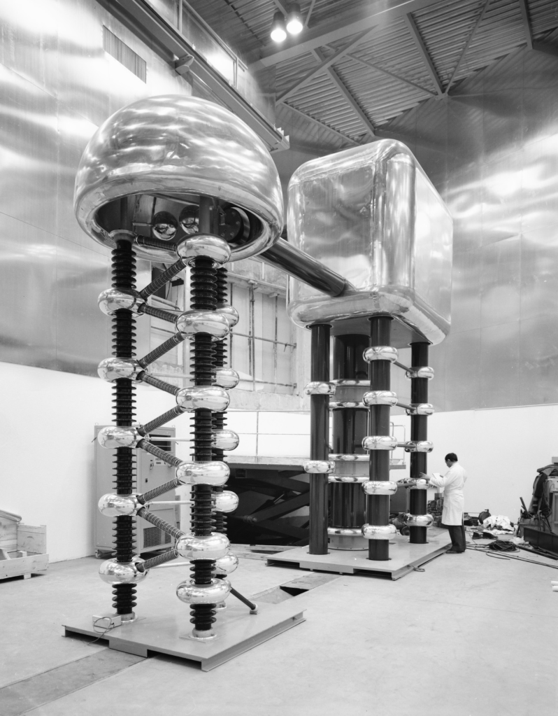
Figure 5. A 750-kV CERN Cockroft-Walton generator is a room-scale machine, about 12 feet (~3 ½ meters) tall, and not a desktop unit. Image credit: CERN.
Common misconceptions
- If the schematic is simple, the layout can be simple: once systems pass about 60 V, safety enters the conversation, and at hundreds and thousands of volts, insulation, spacing, and material behavior dominate.
- Any capacitor and diode rated above the output can be used: each stage sees different voltage and transient stress, so ratings require at least twice the peak voltage across them.
- A multiplier can deliver high voltage and high current from a small stack: many practical uses are low-current, and adding load reduces stored voltage.
- Only the main components need review: small things such as joints, edges, pinholes, and contamination can start discharge.
- Experimental builds are just hobby work: high voltage demands training, protection, and oversight, especially above tens of kilovolts.
Reusable checklist
- Define the target output and verify whether current demand is compatible with 100 mA or less.
- Calculate stage voltages from 120 VAC rms or the chosen source, using 170 V only as the 120 VAC line example.
- Choose parts with reverse ratings that include safety margin, not just nominal voltage.
- Check whether a transformer, flyback stage, or multiplier chain is the better architecture for 10× or 1000× goals.
- Review creepage, clearance, insulation, sharp points, and solder geometry before prototyping.
- Plan overvoltage and overcurrent protection with specialty devices suitable for expected failure energy.
- Use supervised work practices for anything above low-voltage levels, and document discharge paths.
FAQ
What is the difference between a doubler and a multiplier?
A doubler is a specific ×2 case. A multiplier is a ladder that can create ×2, ×3, or ×4 and other stacked peaks when stages are added. The word multipliers is used broadly here.
Why do component voltage ratings grow faster than output voltage?
Each stage is charged from a peak value and then stacked. A 120 VAC line has 170 V peak; a 10× multiple already implies at least 1700 V at the output side, and safety margins such as ×2 or more increase the required part rating.
Is corona only a high-power issue?
No. It depends on local electric field, geometry, surface condition, and insulation quality. That is why ball soldering and smooth construction matter even in modest-current designs.
When should an engineer prefer a transformer path?
When isolation, regulation, efficiency, or power transfer are primary concerns, a transformer or flyback architecture may be more suitable. Multipliers become attractive when the application needs peak stacking from AC or pulsed sources with low current.
References
- Wikipedia entry on flyback converter basics.
- Spellman High Voltage Electronics Corporation high-voltage reference material.
- All About Circuits discussion of voltage multipliers, doublers, triplers, and quadruplers.
- Instructables page showing a high-voltage multiplier build.
- MIT report on the ion-driven aircraft concept.
- MIT Electric Aircraft Initiative article on moving-part-free aircraft propulsion.
- Georgia State University Hyperphysics notes about Cockcroft-Walton accelerators.
- Wikipedia entry on the Cockcroft-Walton generator.
- Wenzel Associates TechLib notes on Cockcroft-Walton voltage multipliers.
- CERN material about the 750 kV Cockcroft-Walton generator and Faraday cage.