
5 Reasons Panel-Level Packaging Moves AI Compute Past Wafer Limits in Electronicseng Semiconductors
Panel formats matter on Electronicseng Semiconductors because AI hardware is expanding advanced packaging toward area, density, and integration limits that circular wafer geometry handles less efficiently. The central issue is whether the manufacturing model can keep pace as compute, memory, and interconnect structures move inside larger packages.
Industry attention is moving toward panel-level processing as one credible answer for the next decade. Lam Research appears in this transition because of long packaging work and investment in panel-level research and manufacturing readiness; the wider story, however, belongs to the whole ecosystem, including the decade ahead of AI infrastructure.
What changes when packaging becomes part of compute performance
Modern AI workloads depend on processors, high-bandwidth memory (HBM), chiplets, and specialized components working as a tightly coupled system. Packaging is no longer a final assembly step that only protects silicon. It is the medium through which bandwidth, latency, energy efficiency, and system scalability are expressed.
When those elements are integrated well, the package behaves like a platform. That matters for training and running large models, because compute and memory are becoming difficult to separate in performance discussions.
The five reasons for the shift
These five reasons explain why panel-level formats are gaining attention.
AI scaling now depends on integrated package behavior
Heterogeneous accelerators combine multiple parts into one package. The practical advantage is not simply putting more dies next to each other. It is making data movement, memory access, and thermal-electrical boundaries behave closer to one system. That supports bandwidth, lower latency, efficiency, and scalability.
Round wafers increasingly fight the geometry of AI packages
Advanced packages are often square or rectangular. As their area grows, a circular wafer wastes more usable space, especially near the edge. The result is a scaling mismatch: designers need more room and denser interconnects, while the substrate shape limits efficient utilization.
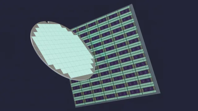 For AI systems that require larger packages, more memory, and faster data movement, panel-level packaging is emerging as a scalable manufacturing path that can extend advanced packaging.
Panels match the shape of advanced packages better
Processing rectangular panels addresses area utilization more directly. This is not just a handling change; it reshapes how large packages can be produced, tested, and routed through manufacturing. Larger substrates provide more room for denser integration and may improve production economics.
Panel formats may pre-empt the next AI bottleneck
Today, many industry observers treat advanced packaging as a priority for investment and innovation. Panel-level processing is attractive because it tackles a scaling constraint before volume demand makes it severe.
The difficulties are real: yield, process control, uniformity, automation, throughput, and standardization remain under development. Achieving fine control over larger substrates requires significant engineering innovation.
The ecosystem is already building the transition
Semiconductor manufacturing shifts usually require equipment suppliers, device makers, packaging houses, researchers, and system designers to move together. Panel-level packaging follows that pattern.
Lam Research has worked on advanced packaging for more than two decades and is investing in research, infrastructure, and ecosystem collaboration. The Salzburg Panel Center of Excellence in Salzburg reflects the direction: accelerate panel research, qualification, and manufacturing readiness while helping customers prepare for future packaging needs.
Quick checklist for semiconductor teams
- Package geometry: Check whether current wafer layouts create edge loss as AI package dimensions grow.
- Interconnect density: Confirm whether the package architecture depends on shorter, denser links between compute and memory.
- Manufacturing readiness: Ask about yield models, process control, uniformity, automation, and throughput rather than only substrate size.
- Standardization: Track qualified flows and industry alignment, because panel transitions depend on shared manufacturing assumptions.
- Ecosystem coordination: Watch equipment, substrate, packaging, and system design collaboration together, not in isolation.
Wafer-level and panel-level packaging: qualitative comparison
| Dimension | Round-wafer packaging view | Panel-level packaging view |
|---|---|---|
| Substrate form | Circular wafer basis | Square or rectangular panel basis |
| Area use for rectangular packages | Loses efficiency as package size grows, especially near edges | Can improve area utilization by matching package shape |
| Scaling pressure | Constrained by wafer limits when AI packages become larger and denser | Offers a path for larger formats and more intricate integration |
| Manufacturing challenge | Existing packaging flows and known process discipline | Needs advances in yield, uniformity, automation, throughput, and standardization |
| Strategic role | Baseline for current advanced packaging | Possible foundation for the next decade of AI packaging scaling |
Data reference: This comparison is qualitative and reflects the reviewed source narrative. It does not introduce new shipment volumes, defect rates, cost figures, or package dimensions.
FAQ
Is panel-level packaging only a larger wafer?
No. It is a manufacturing model change. The substrate geometry affects area utilization, process flow, yield control, automation, and standardization.
Why does AI push packaging forward?
Because AI performance increasingly comes from how processors, HBM, chiplets, and interconnects operate as one package rather than from a single processor alone.
Is the panel shift already proven for volume?
Not fully. Yield, process control, uniformity, automation, throughput, and industry standardization remain active development areas.
What does the source say about Lam Research?
Lam Research is presented as having advanced packaging work spanning more than two decades and investing in panel-level research, infrastructure, and ecosystem collaboration, including the Salzburg Panel Center of Excellence in Salzburg.
Common misconceptions
- Misconception 1: The change is only a size upgrade. In fact, panel-level processing changes how advanced packages are manufactured, qualified, and scaled.
- Misconception 2: Larger area automatically means lower cost. The value depends on yield, uniformity, automation, throughput, and standardization.
- Misconception 3: Packaging is separate from AI compute. Modern AI depends on tightly integrated packages, so packaging choices influence bandwidth, latency, efficiency, and scalability.
Action recommendations
- Engineers should review package area, interconnect density, and HBM placement early, before panel readiness becomes an afterthought.
- Manufacturing and packaging teams should track process control, yield, uniformity, automation, and throughput milestones rather than treating panels as a simple substrate swap.
- Procurement and supply managers should monitor qualified manufacturing flows and ecosystem alignment, because future capacity will depend on shared standards and repeatable production.
- Strategy teams should treat panel-level packaging as a potential next-decade scaling platform, not just an incremental improvement.
Bottom line
Semiconductor history has repeatedly found that compute expansion needs a manufacturing partner. Lithography extended scaling. Advanced packaging helped unlock AI system integration. Panel-level processing now appears as the next candidate for sustaining growth.
For Electronicseng Semiconductors, the takeaway is practical: the AI roadmap is moving package dimensions, memory density, and interconnect complexity toward the edge of circular-wafer limits. The industry is responding with panel formats, ecosystem investment, and manufacturing research. The direction is not finished, but the pressure behind it is clear.