
Electronicseng Semiconductors: CoWoS, AI Packaging Bottlenecks and TSMC Pricing Signals
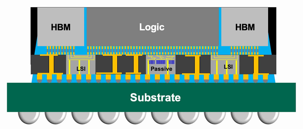
For semiconductor engineers and hardware supply-chain managers, the current CoWoS story is less about a single chip announcement and more about the practical capacity of advanced packaging. CoWoS is TSMC’s advanced packaging solution for high-performance chips: it uses a silicon interposer to place logic dies and high bandwidth memory, or HBM, inside one package. As AI accelerator demand expands, the order book is no longer limited to AI GPUs. Server CPUs and custom ASICs are also pulling the same packaging and test capability, and the resulting unmet orders are lengthening the planning horizon for every team building data-center silicon.
Key signals for Electronicseng semiconductor readers
- CoWoS packaging pressure is spreading from AI GPUs to server CPUs and custom ASICs.
- Equipment lead times have changed from a previous three to six months to a reported six to eight months.
- Nomura estimates that final testing for NVIDIA Blackwell may take about 4 times as long as Hopper, and that Rubin could reach 7 times.
- Taiwan media have reported possible TSMC wafer price increases of about 3% to 6% from January 2027, with 2 nm and 3 nm advanced nodes seen as areas of larger increase.
- TSMC says AI demand is strong and it is accelerating capacity expansion, including 5x reticle area CoWoS packages in production and work toward larger-size solutions and CoPoS.
- GlobalFoundries has signed a multi-year $2 billion manufacturing agreement with TSMC to produce silicon interposers for the TSMC CoWoS supply chain at a New York State plant, with ramp planned for the first half of 2028.
Why the packaging layer has become the choke point
CoWoS is not a simple back-end step. The silicon interposer is the mechanical and electrical backbone that lets a large accelerator combine compute chips with HBM stacks in a short, high-density path. For AI systems, that path affects bandwidth, power delivery, thermal behavior, and package size. When demand moves beyond one product category, the same interposer, assembly, and test resources must serve AI GPUs, server CPUs, and custom ASICs. That broader demand is what turns a packaging technology into a schedule variable.
Testing adds a second constraint. Final test is not just a checkbox; it consumes tester time and labor before a device can move forward. According to the analyst estimate cited in the article, NVIDIA Blackwell final test time is about 4 times Hopper, and Rubin may be about 7 times. If those assumptions hold, more devices and more complex packages can consume capacity even when assembly output rises.
Comparison table: data points, certainty, and impact
| Anchor point | Stated figure | Source tone | What planners should watch |
|---|---|---|---|
| Equipment lead time | From 3 to 6 months to 6 to 8 months | Supply-chain reports | Capacity additions may arrive later than internal plans assumed. |
| Final-test duration | Blackwell about 4 times Hopper; Rubin possibly 7 times | Nomura estimate | Test resources may become a bottleneck alongside packaging lines. |
| Wafer pricing report | About 3% to 6% possible increase from January 2027; 2 nm and 3 nm higher | Taiwan media and supply-chain message, not publicly confirmed | Cost models for AI accelerators and data-center chips may need sensitivity ranges. |
| New packaging capacity | GlobalFoundries multi-year $2 billion agreement; New York State silicon interposer production | Company/signed agreement | Short-term relief is limited because ramp is planned for first half of 2028. |
Where the cost pressure can spread
If TSMC pricing is raised as reported, the immediate exposure sits with products that directly consume CoWoS-style advanced packaging: AI accelerators and data-center chips. These devices combine large silicon area, HBM integration, and test intensity, so packaging cost is not a peripheral line item. Gaming GPUs are different in most cases: they typically do not use this packaging style, so they are not the first product category to feel a CoWoS-specific quote increase.
However, the reported price change is also about wafer foundry pricing, not only packaging. Advanced nodes such as 2 nm and 3 nm are said to see larger increases. If wafer pricing rises, the effect can propagate through other chips and eventually terminal products, even where CoWoS is absent. For product managers, the difference is timing and transmission: packaging costs hit AI hardware sooner; wafer-cost pass-through can be slower and more diffuse.
Common misconceptions
- “All GPUs will see immediate CoWoS-driven price increases.” No. CoWoS-style packaging is central to some AI accelerators, but gaming GPUs typically do not use this packaging, so the direct CoWoS effect is limited.
- “The TSMC price report is confirmed.” No. The pricing item comes from Taiwan media and supply-chain reporting; TSMC has not publicly confirmed the specific increase.
- “Test time is only a quality issue.” Not anymore. Final test consumes capacity. If Blackwell takes about 4 times as long as Hopper and Rubin reaches 7 times in the analyst estimate, test time can tighten availability as much as line space.
- “New capacity solves the current squeeze quickly.” The GlobalFoundries agreement is meaningful for supply-chain resilience, but ramp is planned for first half of 2028, so it does not materially ease a near-term bottleneck.
- “CoPoS and 5x CoWoS are the same thing.” They are different points on a roadmap. 5x-reticle-area CoWoS is in production, while CoPoS is being advanced and may change future large-package assembly approaches.
FAQ for semiconductor readers
What exactly is CoWoS doing in an AI chip?
CoWoS uses a silicon interposer to connect compute chips and HBM in a single package. It shortens the electrical path, supports high bandwidth, and allows AI accelerators to reach the package scale required by data-center workloads.
Why would a packaging issue affect server CPUs and custom ASICs?
Because advanced packaging capacity is shared. When AI GPUs expand demand, server CPUs and custom ASICs that also need advanced packaging compete for interposer and assembly resources. The backlog grows when multiple product families draw from the same constrained flow.
Does the GlobalFoundries and TSMC deal change U.S. manufacturing assumptions?
It adds a multi-year $2 billion manufacturing link for silicon interposers tied to the TSMC CoWoS supply chain in New York State. It matters for supply-chain geography, but the planned ramp in first half of 2028 means it is not a short-term capacity answer.
Should procurement teams treat the pricing rumor as a cost certainty?
No. Treat it as a risk range because the report is not confirmed. A safer planning method is to model an increase of about 3% to 6% for relevant wafer pricing, with attention to 2 nm and 3 nm nodes, while tracking official disclosures.
What is the difference between packaging capacity and test capacity?
Packaging capacity is about assembly, interposers, and line throughput. Test capacity is about tester time, validation, and yield screening before shipment. The current reports suggest both can constrain AI hardware schedules, especially when test duration rises to 4 times or 7 times in the Nomura estimate.
Action recommendations for engineering and supply-chain teams
- Separate packaging risk from test risk in project plans, because CoWoS capacity and final-test duration are not interchangeable constraints.
- Use the reported 6 to 8 month equipment lead time as a sensitivity input for capacity forecasts that previously assumed 3 to 6 months.
- Model AI accelerator cost exposure under the possible about 3% to 6% wafer pricing change, especially for 2 nm and 3 nm assumptions, without treating the rumor as confirmed.
- Review whether products use CoWoS-style packaging; if they do, prioritize schedule and cost visibility. If they do not, focus more on wafer-price pass-through rather than direct CoWoS quotes.
- Ask suppliers for clearer timing around test capacity, not only assembly capacity, since final test may take about 4 times as long for Blackwell versus Hopper and possibly 7 times for Rubin.
- Track 5x-reticle-area CoWoS mass production, larger-size package development, and CoPoS progress as signs that package scale, not only die size, is rising.
- Treat the GlobalFoundries New York State interposer plan as a longer-term supply-chain resilience signal, with the first half of 2028 ramp as the practical timing anchor.
Bottom line for Electronicseng readers
CoWoS has moved from a manufacturing detail to a semiconductor planning variable. For AI accelerators, the near-term pressure comes from packaging and test capacity; for broader products, the possible wafer price increase reported for January 2027 creates a cost transmission path. Engineering and procurement teams should avoid overreacting to a single rumor, but they should also avoid treating packaging, testing, and wafer cost as independent line items. In a tight AI supply chain, they can bind together.