
From Specification to Verified GDS: A Semiconductor Engineer's Framework for Evaluating AI Agents — Electronicseng
By Rachel Williams, Electronics & Engineering — Electronicseng Semiconductors column
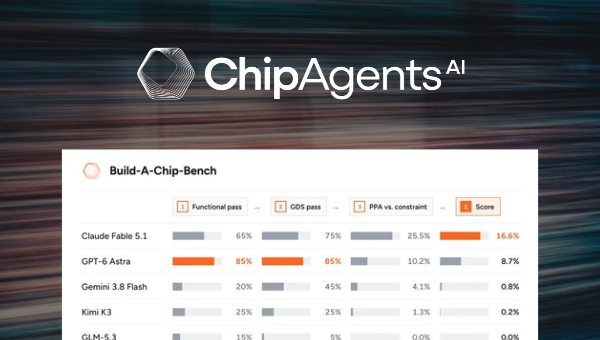
For a team shipping custom silicon, the useful question about an AI agent is not whether it can emit syntactically valid RTL. It is whether the decisions embedded in that RTL still hold after verification, synthesis and physical implementation — all the way to a verified Graphic Design System (GDS) stream that could actually be handed forward. That distinction between a demonstration and an engineering result is the design principle behind Build-A-Chip-Bench, the evaluation suite ChipAgents developed with NVIDIA to score AI agents across the end-to-end digital IC design flow, from specification through physical implementation and verified GDS. Every task is built to connect individual design steps to a measurable engineering outcome rather than a task-level grade.
The pressure behind this reframing is structural rather than fashionable. Physical AI, data centers, automotive systems and edge devices all require architectures tuned to particular workloads, memory bandwidth, latency and energy efficiency, so demand for custom silicon keeps climbing while teams coordinate heterogeneous compute blocks, complex interconnects and multiple domains against increasingly demanding power, performance and area (PPA) targets. AI is already inside that workflow: design and verification engineers apply it to generate test cases, assist debugging and implement portions of RTL. What remains unproven is coverage of the whole flow — and that is a measurement problem before it is a model problem.
Benchmark landscape: isolated tasks versus a complete flow
CVDP and ChipBench advanced AI for chip design by offering common tasks on which systems could be evaluated and compared. Comparison is precisely where their usefulness now flattens: as frontier models improve, more demanding evaluations are needed to distinguish progress on individual tasks from the ability to execute a complete design flow.
Build-A-Chip Bench responds by raising two variables simultaneously — task difficulty and end-to-end scope. It asks agents to carry a design from workload specification through final GDS, linking stages that narrower benchmarks evaluate in isolation. Correct RTL generation alone is not enough. An agent must preserve functional correctness, satisfy PPA constraints, and resolve the problems that emerge during synthesis and physical implementation.
| Evaluation layer | Unit of assessment | What a good score establishes | Constraint described in the source material |
|---|---|---|---|
| CVDP | Individual design tasks shared across systems | Relative capability on isolated steps | Scores plateau near 65–70%, with many remaining tasks appearing to have quality issues — ambiguous specifications or malformed testbenches — limiting measurable headroom |
| ChipBench | Individual design tasks shared across systems | Relative capability on isolated steps | Task-level results do not show whether a full flow can be executed end to end |
| Build-A-Chip Bench | Specification-to-GDS execution by an agent | Functional correctness, PPA satisfaction and resolution of synthesis and physical-design issues in one chain | Requires managing architecture, RTL, verification and physical-design dependencies in a single run |
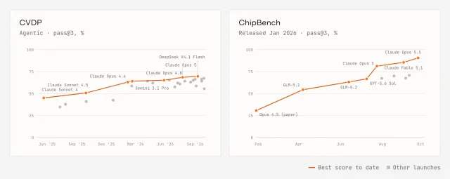
Figure 1 — Reported pass@3 results for CVDP and ChipBench. CVDP scores plateau near 65–70%, and much of the apparent ceiling comes from task quality issues such as ambiguous specifications or malformed testbenches, which cap the headroom any benchmark can reveal. The best score to date is drawn with orange lines; other model launches appear as gray markers.
Scale, roles and inputs: what a reference task actually contains
Read the benchmark as a scope definition rather than a leaderboard. At moderately large scale — designs of 100K-5M standard cells — the tasks exercise a representative specification-to-GDS flow and the dependencies across architecture, RTL, verification and physical implementation. In industry these activities typically involve teams of architects, RTL designers, design verification (DV) engineers, physical design (PD) engineers, EDA engineers, and more. The benchmark requires a single agent to manage the technical dependencies across those disciplines.
What each task hands to the agent:
- A workload specification and a fixed interface
- An open-source EDA environment
- Constraints whose achievability is established by reference designs
- Hidden verification IP that evaluates functional behavior against held-out tests
- A separate grader that evaluates the final submission
What the agent must own without a hand-off:
- Architecture and microarchitecture decisions
- RTL development, plus the testbenches that prove it
- Verification against the hidden checks rather than against self-authored ones
- Physical implementation, including EDA flow scripts and manual floorplanning and placement as needed
Worked example: an INT4 inference accelerator under pinned constraints
One representative task makes the difficulty concrete. An INT4 inference accelerator for Qwen3-0.6B must be built using Verilator, OpenSTA, OpenROAD, and Nangate45 PDK. The datapath architecture, buffering and scheduling are all chosen by the agent; the constraint envelope is not negotiable.
| Parameter | Requirement in the task | Engineering consequence |
|---|---|---|
| Workload | INT4 inference accelerator for Qwen3-0.6B | Data-format and throughput targets are set before RTL exists |
| Toolchain | Verilator, OpenSTA, OpenROAD, Nangate45 PDK | An open-source flow with a fixed PDK, so results are reproducible across submissions |
| Timing | 400 MHz | Clocks cannot be traded away late without reopening RTL and floorplan choices |
| Area | fit within 6 mm² | Macro count and buffering decisions feed directly into routability |
| Throughput | at least 15 decode tokens per second | Decode-rate targets make scheduling a first-class architectural choice |
| Power | less than 10 W | Energy is a hard gate, not a post-hoc report metric |
| Memory bandwidth | pinned at 12.8 GB/s | The agent must design around a fixed bandwidth budget instead of relaxing it |
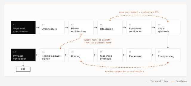
Figure 2 — A representative specification-to-GDS flow with feedback paths. Note the caveat carried in the source: the benchmark checks do not establish production signoff.
Scoring mechanics: two gates first, PPA second
Fixed open-weight harnesses were used to evaluate all models, which keeps the comparison honest across vendors. To pass, a design must clear two independent gates: functional verification against the hidden VIP, and a physical gate requiring a routed GDS layout with no hold-time or design-rule violations. Designs that pass both gates are scored on PPA relative to task constraints, while failures receive zero. The overall score is the average across all tasks — a structure that punishes a beautiful but unverifiable design exactly as harshly as an unverifiable one.
Data citation: what the first model runs returned
The published numbers are best read as directional evidence about flow discipline, not about model ranking.
| Model | Functional pass rate | GDS pass rate | Overall score | Reading for engineers |
|---|---|---|---|---|
| Claude Fable 5.1 | 65% | 75% | 16.6% (highest overall) | PPA converted passing designs into score |
| GPT-6 Astra | 85% (led both pass rates) | 85% | 8.7% | A lower PPA score erased the pass-rate advantage |
These preliminary results do not establish production signoff or silicon validation.
Three failure modes that decide whether an agent converges
1. Optimization that costs you verified behavior. Useful engineering judgment appears alongside inconsistent completion. One run showed an agent applying a post-route engineering change order (ECO), resizing one instance to eliminate a remaining slew violation, then passing final-netlist equivalence checks. Yet attempts to improve PPA can introduce functional regressions and consume the remaining time budget in debugging.
2. Architectural fixes deferred until the routing loop is exhausted. Architectural corrections can also be delayed while physical-design parameters are adjusted. One run showed an agent documenting a storage change that would reduce SRAM macros from 51 to 27, deferring it, and spending roughly six hours trying routing configurations before implementing it. Effective closure requires tracing physical failures back to the design decisions that produced them.
3. Tool runtime as the real budget. Iteration is limited by tool runtime. A single place-and-route run can exceed four hours, so agents must prioritize changes and reserve sufficient time for final verification and implementation.
The score plateaus in these sample runs reflect the same three failure modes: functional regressions during optimization, delayed architectural corrections, and slow tool loops that stall further improvement (Figure 3).
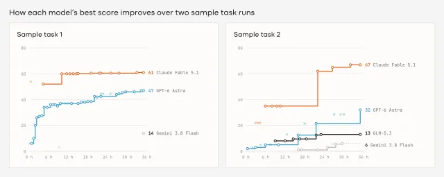
Figure 3 — Best agent-measured scores so far on two sample tasks during the first 36 hours of 72-hour runs, before hidden-VIP grading. Saved designs appear as circles and failed attempts as crosses; best-so-far curves do not show every intermediate regression, and models absent from a panel produced no passing design on that task.
Checklist: what your own agent evaluation should measure
- Does the agent preserve verified behavior while it optimizes for PPA?
- Does it identify the architectural cause of a physical failure, or only patch the symptom?
- Does it allocate runtime effectively, given that one place-and-route pass can exceed four hours?
- Does work completed at one stage remain valid in the next stage, or does each stage invalidate its predecessor?
- Are functional correctness and the routed-GDS physical gate both cleared before any score is discussed?
- Are PPA results reported relative to task constraints, with failures recorded as zero rather than as partial credit?
Common misconceptions to retire
- Functional correctness equals a finished design. The benchmark treats it as one of two gates: a routed GDS layout with no hold-time or design-rule violations is also required, and PPA is scored only after both are cleared.
- A high pass rate is a high score. GPT-6 Astra led both pass rates at 85% yet landed at 8.7% overall because of a lower PPA score.
- Benchmark success is production signoff. The benchmark checks do not establish production signoff, and the preliminary results do not establish silicon validation.
- A plateau always means the model is the limit. For CVDP, many remaining tasks appear to have quality issues — ambiguous specifications or malformed testbenches — which limits measurable headroom.
- An end-to-end benchmark reproduces a real program. Although the benchmark spans the design flow, it captures only part of the complexity of a production silicon program.
Action recommendations for semiconductor teams
- Treat specification-to-GDS capability, not single-step generation, as the acceptance criterion when evaluating agent tooling; isolated task wins do not prove flow execution.
- Instrument the transition between stages in your own trials: keep records of which optimization produced a functional regression, and which routing failure traced back to an architectural decision.
- Build time budgets around tool loops. With a single place-and-route run that can exceed four hours inside a 72-hour window, reserve capacity for final verification and implementation instead of chasing PPA.
- Pin constraints the way the benchmark pins them — fixed interface, fixed bandwidth, achievable targets established by reference designs — so agent behavior is comparable across runs.
- Keep engineers guiding design decisions and validating the resulting implementations; the demonstrated capabilities point to substantial potential for AI-assisted silicon design precisely because that division of labor holds.
FAQ
What is Build-A-Chip-Bench and who built it?
ChipAgents developed Build-A-Chip-Bench with NVIDIA to evaluate AI agents across the end-to-end digital IC design flow, from specification through physical implementation and verified Graphic Design System (GDS), using realistic, demanding tasks that connect individual design steps to a measurable engineering outcome.
How does it differ from CVDP or ChipBench?
CVDP and ChipBench provide common tasks for evaluating and comparing systems on individual steps. Build-A-Chip Bench adds task difficulty and end-to-end scope, requiring an agent to carry a design from workload specification through final GDS while preserving functional correctness, satisfying PPA constraints and resolving synthesis and physical-design issues.
What does a single task give the agent?
A workload specification, a fixed interface and an open-source EDA environment. Achievable constraints are established by reference designs, hidden verification IP evaluates functional behavior against held-out tests, and a separate grader evaluates the final submission.
How is a submission judged as a pass?
Two gates must both be cleared: functional verification against the hidden VIP, and a physical gate requiring a routed GDS layout with no hold-time or design-rule violations. Passing designs are then scored on PPA relative to task constraints; failures receive zero, and the overall score is the average across all tasks.
Are these results proof that an agent can tape out?
No. The preliminary results do not establish production signoff or silicon validation, and the benchmark captures only part of the complexity of a production silicon program. Under the tested toolchain and resource budgets, frontier agents demonstrated the ability to execute the specification-to-GDS flow but still struggled to preserve correctness and converge on strong PPA.
The take for design and supply-chain readers
For engineering teams, evaluation should therefore measure whether agents preserve verified behavior during optimization, identify architectural causes of physical failures, and allocate runtime effectively, with work completed at any stage remaining valid in subsequent stages. Read this way, the benchmark is less a scoreboard than a specification for how semiconductor organizations should test agent tooling before committing schedule to it — and a reminder that in the current generation of results, the decisive gap sits between a passing design and a good one.
Editorial contact: Electronics & Engineering, Electronicseng — info@electronicseng.com.