
Electronicseng Analysis: 4F² DRAM Transition, ChangXin Validation, and the 3D Memory Roadmap
For the electronics and semiconductor audience followed by Electronicseng, the signal in this disclosure is not simply that a new memory format has been named. It is that a platform can enter wafer-level qualification before commercial release. The reported completion of ChangXin engineering sample validation indicates that core performance targets for the 4F² platform have reached design expectations on real wafers. The remaining step before large-scale production is customer verification; once that verification closes, the manufacturing process can move into volume execution.
The product context is also specific. A prior public statement from ChangXin pointed to a year-end timing for a new DDR5 RDIMM aimed at the server domain, an area described as one of the most difficult application fields. That product is said to integrate 4F² advanced technology.
Global positioning: validation, direction-setting, and possible first deployment
The disclosed timeline gives the comparison its edge. Samsung and SK hynix have both identified 4F² as a key direction for below the 10nm class, while ChangXin is reported to have completed engineering sample validation ahead of those disclosed milestones. If later verification and production activities proceed as planned, ChangXin could become the first company worldwide to realize 4F² in a practical deployment.
Technical logic: why 4F² matters beyond a geometry label
DRAM scaling has always been organized around density: the wafer must carry more memory units inside a comparable footprint so that cost per bit can continue to fall. The reported 4F² path is important because it is framed as a mechanism that helps break the bottleneck in DRAM unit shrinkage and supports movement toward 3D DRAM.
Once DRAM enters the 10nm class, the long-standing 6F² cell is no longer easy to sustain because it is close to physical limits. The IEEE International Roadmap for Devices and Systems (IRDS) frames the choice plainly: when half-pitch scaling becomes increasingly difficult, “the transition from 6F² to 4F² cells is the most promising path to sustain the cost trend”.
Cell geometry and platform signals
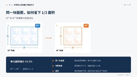
The clearest parameter is area. A 4F² unit is described as 2F×2F, where F represents the minimum line width or spacing achievable by lithography. This is about two-thirds of the area of a mainstream 6F² unit. The geometry explains why 4F² has become a common selection among leading storage makers.
Two major industry signals reinforce that view. SK hynix has placed its 4F² vertical-gate platform and 3D DRAM side by side as two major technology pillars. Samsung published a 10nm-class 4F² paper at ISSCC 2026, and its chief technology officer confirmed this October that the company is also developing the same direction. More broadly, 4F² is treated as a necessary stage on the route to 3D DRAM.
ChangXin architecture: VSG transistor and process decoupling
Within the reported ChangXin 4F² architecture, the central device element is a self-developed VSG transistor, meaning vertical surrounding gate. Because the gate exerts stronger control over a vertically surrounding channel, short-channel effects and leakage can be reduced.
The platform is not only a transistor change. The process architecture separates DRAM and CMOS manufacturing, then links them with wafer-level hybrid bonding for high-speed interconnect. This decoupling allows logic performance, storage density, and reliability to be optimized independently, rather than requiring all three to be satisfied through a single blended sequence.
Cited anchors used in this Electronicseng analysis
- IEEE International Roadmap for Devices and Systems (IRDS): “the transition from 6F² to 4F² cells is the most promising path to sustain the cost trend”.
- ISSCC 2026: cited as the conference venue for the Samsung 10nm-class 4F² paper.
- Company confirmation: a chief technology officer statement this October regarding Samsung development activity.
- Platform positioning: SK hynix 4F² vertical-gate and 3D DRAM listed as two major technology pillars.
- Product timing: ChangXin public statement pointing to year-end DDR5 RDIMM for the server field.
Comparison: 6F² baseline and 4F² transition
| Dimension | Reported 6F² status | Reported 4F² status |
|---|---|---|
| Cell area | Mainstream 6F² unit is the reference point that becomes hard to sustain in the 10nm class. | 4F² is described as 2F×2F, about two-thirds of 6F² area. |
| Roadmap role | Approaches physical limits under the density-and-cost logic described in the source. | Presented as a path that helps break unit-scaling difficulty and supports movement toward 3D DRAM. |
| Cost interpretation | Difficulty of sustaining cost trend grows as half-pitch scaling becomes harder. | IRDS quote: “the transition from 6F² to 4F² cells is the most promising path to sustain the cost trend”. |
| Manufacturer signals | Historical mainstream geometry. | Samsung, SK hynix, and ChangXin signals include a below the 10nm class direction, ISSCC 2026 paper, two major technology pillars, and engineering sample validation. |
| Maturity evidence | Not described as the subject of the disclosed new milestone. | ChangXin reported to have completed engineering sample validation; year-end server DDR5 RDIMM remains tied to subsequent client verification. |
Checklist: items that determine whether the milestone becomes deployment
- Track customer verification after engineering sample validation, because volume production is described as starting only after that stage.
- Watch the year-end server-oriented DDR5 RDIMM statement as a concrete product test of the 4F² integration claim.
- Compare disclosed maturity levels: completed engineering sample validation, direction setting in below the 10nm class, conference paper, and executive confirmation.
- Review how 2F×2F area, two-thirds relative to 6F², affects density assumptions in cost-per-bit models.
- Examine whether VSG and wafer-level hybrid bonding are presented as qualification evidence rather than architecture description only.
FAQ: the decision-relevant questions
Does completed engineering sample validation mean the product is already qualified?
No. The disclosed condition says core performance targets have been met on real wafers. Large-scale production is still described as beginning after client verification is completed.
Is 4F² a substitute for 3D DRAM?
No. 4F² is framed as a route that helps solve unit-scaling difficulty while supporting movement toward 3D DRAM. It is positioned as a stage or platform path, not as a completed replacement for 3D DRAM.
Why does the transition from 6F² to 4F² matter commercially?
Because DRAM economics depend on continuing to integrate more units on the same wafer. The IRDS statement connects the 6F²-to-4F² transition to maintaining the cost trend when half-pitch scaling becomes harder.
What is the role of VSG in the ChangXin case?
VSG, or vertical surrounding gate, is described as the core self-developed transistor element. Its vertical channel surround is presented as stronger gate control, helping mitigate short-channel effects and leakage.
Why is hybrid bonding mentioned?
The architecture separates DRAM and CMOS process flows and then uses wafer-level hybrid bonding for high-speed interconnect. That allows logic performance, density, and reliability to be optimized as separate variables.
Common misconceptions
- Area reduction is not the same as confirmed cost reduction. The disclosed statement supports a cost-trend path, not a guaranteed cost outcome.
- Not every 4F² reference represents the same maturity. The available evidence ranges from direction statements to a paper, an executive confirmation, and engineering sample validation.
- VSG does not stand alone. The reported architecture also involves decoupling DRAM and CMOS manufacturing and connecting them through wafer-level hybrid bonding.
- The server DDR5 RDIMM reference is a stated target tied to the 4F² story, not an automatic confirmation that all qualification steps are complete.
Action recommendations
- For procurement teams: treat the year-end DDR5 RDIMM statement as a schedule signal, while waiting for client verification evidence before assuming volume supply.
- For system designers: separate memory architecture assumptions into wafer validation, client qualification, and production readiness before committing to roadmap content.
- For analysts: compare the disclosed evidence layers across ChangXin, Samsung, and SK hynix without collapsing them into one claim of equivalent maturity.
- For technology planners: use the 2F×2F geometry, the IRDS cost-trend statement, and the VSG plus hybrid-bonding architecture as the concrete checkpoints for assessing the move toward 3D DRAM.
The practical takeaway for Electronicseng readers is that the story has moved from a terminology debate to an evidence sequence: wafer validation, customer verification, server-oriented product timing, and production readiness. The 4F² label is still tied to the larger 3D DRAM path, but the next judgment should be based on how each disclosed step converts into qualified delivery rather than on the milestone language alone.