
Semiconductor Supply Watch: CXMT HBM3E Timeline, Yield and China AI Memory Risk
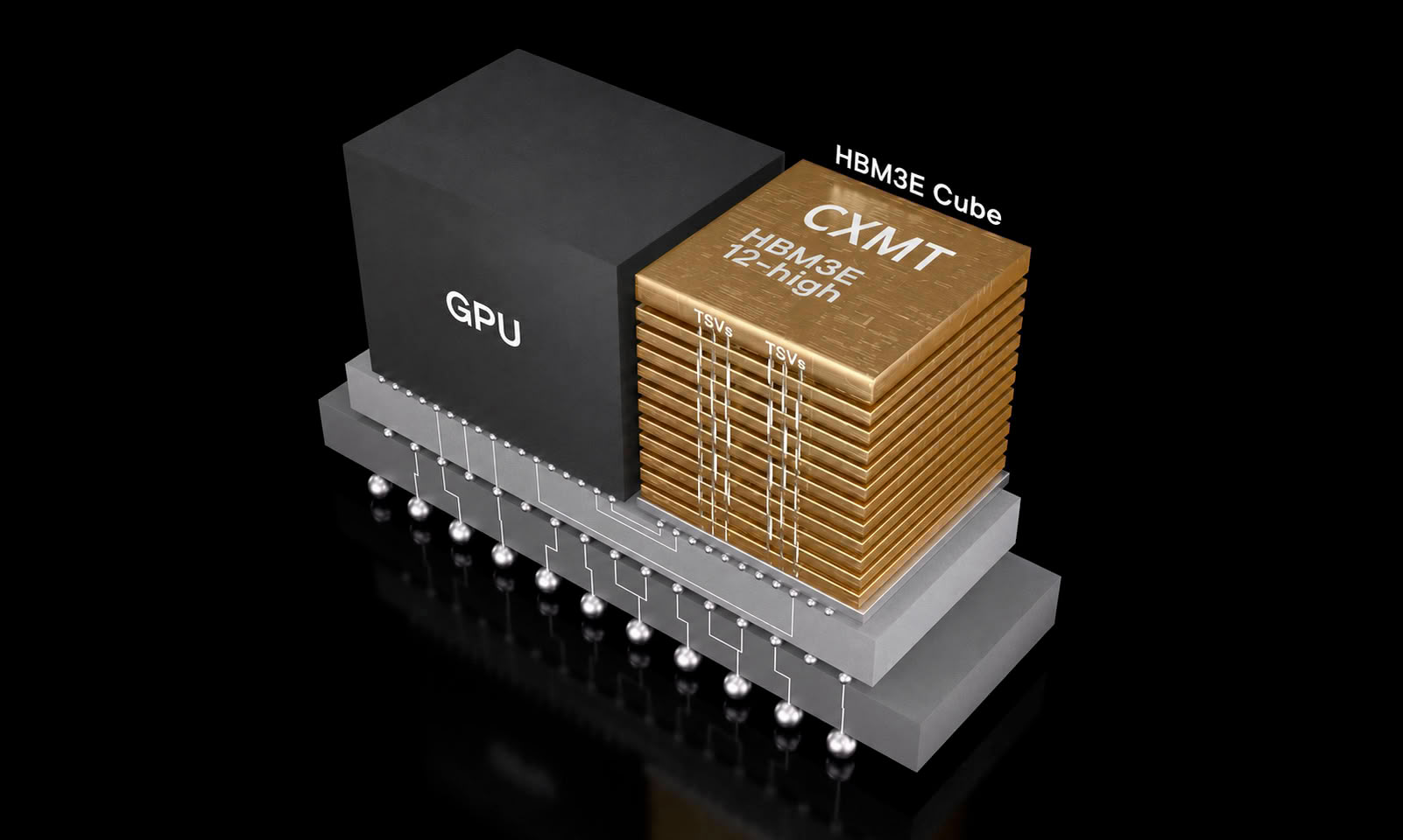
ChangXin Memory Technologies (CXMT) is reported to be preparing HBM3E mass-production introduction within the next two months, with a formal production window pointed before the end of 2026. The company already started risk production this August and delivered samples to selected customers, so the local China AI memory path is moving from trial line toward commercial qualification.
Why CXMT HBM3E Matters for Semiconductor Design Teams
AI accelerators, data-center GPUs and high-performance computing systems rely heavily on HBM because it offers much higher bandwidth than traditional DRAM and therefore supports training and running large AI models. The global HBM market is currently dominated by SK Hynix, Samsung Electronics and Micron, which makes a new qualified supplier important for China's AI hardware ecosystem, especially when supply pressure and import restrictions raise the value of local sourcing.
For engineering managers, the story is not only a market-news item. It is a selection question: can a locally available HBM3E device meet JEDEC electrical assumptions, stack capacity expectations, packaging reliability and customer-validation evidence before a product team locks a memory architecture?
HBM3E Parameter Checklist
The following checklist reflects the JEDEC-based parameters mentioned in the source information and should be verified against actual datasheets and sample reports before design-in.
- Bus architecture: confirm the device is specified as HBM3E under the JEDEC 1024-bit framework.
- Pin rate range: check whether the target configuration falls between 9.2Gbps and 12.4Gbps, with common values near 9.6Gbps.
- Bandwidth budget: validate the approximately 1.2TB/s system-level assumption under the selected stack and rate.
- Capacity options: compare 24GB through 36GB configurations against accelerator memory footprint needs.
- Stack form: track both 8-layer stack and 12-layer stack options, but note that CXMT is expected to concentrate on 8-stack HBM3E first.
- TSV interconnect: require documentation for through-silicon via count, alignment control, thermal behavior and reliability qualification.
- Customer qualification: distinguish standard samples from yield-optimized versions and obtain test status from each customer.
Yield and TSV Constraints Behind the Timeline
HBM3E production is not only a wafer-fab challenge. Multi-layer DRAM dies must be vertically stacked through TSV silicon via technology, and that combination of manufacturing and packaging raises the yield threshold. The source information places CXMT's overall HBM3E yield at about 20% to 30%, compared with the leading international vendors. Front-end wafer manufacturing yield is reported at about 30%. After entering back-end packaging, the pass rate may improve by about 70%, yet the final overall yield still needs additional improvement.
TSV maturity appears to be the sharpest constraint. In the reported cases, Samsung used about 5000 TSV connections per layer during the HBM2 era, while SK Hynix exceeded 8000 TSV in its HBM3 products. CXMT, by contrast, is reported to try an HBM3E design with about 3000 TSV. Fewer TSV paths may reduce some assembly complexity, but it also requires higher precision and reliability controls to meet HBM3E performance expectations.
Comparison of Reported Production Readiness Signals
| Signal | CXMT reported status | Reference point in the source information | What it implies for a semiconductor plan |
|---|---|---|---|
| Mass-production window | Prepared to bring HBM3E into mass production within the next two months, targeting before the end of 2026 | Global market led by SK Hynix, Samsung Electronics and Micron | Treat the date as a production-readiness milestone, not as proof of sustained volume supply |
| Yield profile | Overall yield approximately 20% to 30%; front-end about 30%; back-end pass-rate improvement about 70% | Leading vendors are not given a numeric yield in the source, but are implied as the benchmark gap | Ask for yield breakdown by wafer, stack and packaging lot |
| TSV density | About 3000 TSV attempted for HBM3E | Samsung HBM2 about 5000 TSV; SK Hynix HBM3 over 8000 TSV | Validate power delivery, interconnect reliability and test coverage |
| Stack priority | Focus expected on 8-stack HBM3E; 12-stack not advanced quickly | HBM3E mainstream forms include 8-layer stack and 12-layer stack | Plan memory capacity and bandwidth with 8-stack assumptions first |
| Customer samples | Two versions delivered: standard version and yield-optimized version | Customers are testing and verifying samples | Require version-controlled reports; performance claims must be tied to sample revision |
| Market entry | Domestic AI accelerator products using CXMT HBM3E may enter market in 2027 if validation goes well | Technology gap remains one to two generations compared with global leaders | Consider HBM sourcing as a staged qualification path, not immediate replacement |
Sample Status and Performance Positioning
According to the source information, CXMT has sent two versions of HBM3E samples to domestic AI chip companies. One is a standard version, and another is a yield-optimized version. They are currently under customer-side testing and validation. Initial performance data reportedly place the current CXMT HBM3E product closer to SK Hynix's previous-generation HBM3 than to the more advanced international HBM3E offerings.
Still, for a vendor that has only entered the HBM field, reaching mass-production readiness itself is a major breakthrough. The strategic importance is especially visible in China, where AI chip makers need high-bandwidth memory capacity and where supply tightness plus import restrictions create strong demand for alternative HBM sources. Recent AI chip price increases have been widely attributed in part to high-bandwidth memory supply pressure. Companies such as Alibaba T-Head and Cambricon have been reported to test domestic HBM solutions to reduce dependence on overseas supply chains.
Common Misconceptions
- "Within the next two months equals shipping-equal maturity." The reported schedule describes a mass-production introduction plan. Yield improvement and customer qualification remain conditions that can move commercial availability.
- "A 70% back-end pass-rate improvement means total yield becomes high." The source separates front-end, back-end and final overall yield. Final overall yield still needs improvement.
- "Performance close to previous-generation HBM3 means no HBM3E value." The comparison is a benchmark gap, not a product-use verdict; 8-stack HBM3E can still serve as a local supply option and a validation milestone.
- "A 12-stack roadmap is already solved." The source says CXMT is expected to focus on 8-stack HBM3E in the short term and will not quickly push the larger-capacity 12-stack version.
FAQ
When is CXMT planning to start HBM3E mass production?
The reported plan is to start within the next two months, with the formal production window aimed at before the end of 2026.
What HBM3E parameters are specified in the source?
The source refers to JEDEC HBM3E standards using a 1024-bit bus architecture, a pin transfer rate between 9.2Gbps and 12.4Gbps, common configuration around 9.6Gbps, total bandwidth about 1.2TB/s, and capacity options from 24GB to 36GB in 8-layer stack and 12-layer stack forms.
Why is yield the main issue?
HBM3E requires multi-layer DRAM die stacking through TSV technology, which makes manufacturing and packaging difficult. Reported overall yield is about 20% to 30%, while final commercial volume depends on further improvement.
How does CXMT's TSV approach differ from the reported vendor examples?
Samsung used about 5000 TSV per layer in the HBM2 era, SK Hynix exceeded 8000 TSV in HBM3 products, while CXMT is reported to try about 3000 TSV for HBM3E design.
When could domestic AI accelerators with CXMT HBM3E appear?
If customer validation proceeds smoothly, the source indicates that domestic AI accelerator products using CXMT HBM3E could enter the market as soon as 2027.
Action Recommendations for Engineers and Procurement Teams
- Request the sample version map: distinguish the standard sample from the yield-optimized sample and require test reports for each revision.
- Validate stack assumptions against system bandwidth: calculate memory capacity, thermal envelope and board-level power using 8-stack HBM3E as the near-term baseline.
- Ask for TSV count and qualification data: compare the reported 3000 TSV design against the 5000 TSV Samsung HBM2 and over 8000 TSV SK Hynix HBM3 examples, focusing on reliability rather than count alone.
- Build a supply-risk model around yield, not only the production date: track the 20% to 30% overall yield, 30% front-end yield and 70% back-end pass-rate improvement as separate variables.
- Review customer-test visibility from AI chip partners: monitor reported validation activities involving Alibaba T-Head and Cambricon as leading demand-side signals.
- Plan a staged adoption path: treat CXMT HBM3E as an emerging China supply option while preserving established HBM sources until one to two generations of performance, volume and reliability gaps are closed.
Data Reference
All quantitative anchors below are carried from the audited source information and are included here without modification, except for translation into English.
- Timeline: within the next two months; before the end of 2026; risk production this August; possible market entry in 2027.
- HBM3E electrical specification: 1024-bit bus; 9.2Gbps to 12.4Gbps pin transfer rate; common 9.6Gbps; about 1.2TB/s bandwidth.
- Memory configuration: 24GB to 36GB; 8-layer stack and 12-layer stack; near-term CXMT focus on 8-stack.
- Yield and process: overall yield about 20% to 30%; front-end yield about 30%; back-end pass-rate improvement about 70%.
- TSV comparison: Samsung HBM2 about 5000 TSV; SK Hynix HBM3 over 8000 TSV; CXMT HBM3E about 3000 TSV.
- Market context: SK Hynix, Samsung Electronics and Micron lead global HBM; Alibaba T-Head and Cambricon test domestic HBM; technology gap remains one to two generations.
Written by Rachel Williams, Electronics & Engineering. Contact: info@electronicseng.com