
Electronicseng Semiconductors | Goodram Industrial Memory Validation in Poland: Parameters, BOM Stability, and IIoT Reliability
In embedded computers and industrial IoT nodes, memory and storage are not simple line items on a schematic; they determine whether a controller, process recipe, or field gateway behaves predictably over years. For Electronicseng’s semiconductor audience, the useful question is not whether a DRAM module or SSD exists, but whether it can be screened, qualified, and sourced with enough engineering evidence to reduce latent failures on the production floor. The quality operations associated with Goodram in Łaziska Górne, Poland, provide a practical case study: technology-specific stress tests, environmental chamber trials, and configuration control aimed at industrial reliability.
Reliability, OEE, and TCO: Where Memory Validation Fits in Industrial Computing
Industrial designers usually evaluate subsystems through Overall Equipment Effectiveness and Total Cost of Ownership. A failed SSD or DRAM part may be low in unit price but expensive in downtime, dispatching a technician, losing traceability data, or restarting a line. Because embedded platforms often run continuously, a defect that appears only after thermal soak, voltage variation, or repeated host-controller negotiation may not be exposed by routine assembly testing.
This is why semiconductor procurement teams ask suppliers for more than datasheets. They need evidence about burn-in conditions, host coverage, batch-to-batch consistency, and long-term BOM control. They also need a manufacturing route that can communicate with engineering and quality assurance quickly when an interface marginality or firmware anomaly appears.
Test Architecture: Matching Screening Methods to Failure Physics
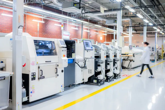
Uniform testing across all products is inefficient. It increases throughput cost and, for flash-based devices, may consume endurance before shipment. Goodram’s approach therefore separates DRAM and SSD validation according to the failure mechanisms likely to be accelerated by the specific technology.
DRAM Screening: Heat, Host Diversity, and Address Mapping
In DRAM modules, higher temperature increases charge leakage and can reveal weak retention, marginal refresh, or timing sensitivity. In this workflow, modules are operated under full load at 80°C, with temperature measured at component surfaces rather than only at the chamber or board point. Depending on the selected procedure, a stress run may last between 30 and 180 minutes.
Compatibility is another constraint because memory controllers in industrial PCs are not homogeneous. The test farm includes more than 400 diagnostic platforms and more than 400 computer platforms based on Intel and AMD architectures. This breadth supports verification across different DRAM generations, including ECC and Registered DIMM configurations commonly used when error correction and large module capacity matter.
Workload generation is not left to general-purpose benchmarking tools. Proprietary in-house software uses low-level routines written in assembly language and SSE/MMX instructions to create complex read/write traffic, including random and sequential access patterns. The test architecture also maps logical addresses to physical silicon structures, so a failure can be traced to a particular DRAM die. That traceability feeds root-cause analysis and manufacturing feedback.
SSD Screening: Endurance-Aware Coverage of the Whole Address Space
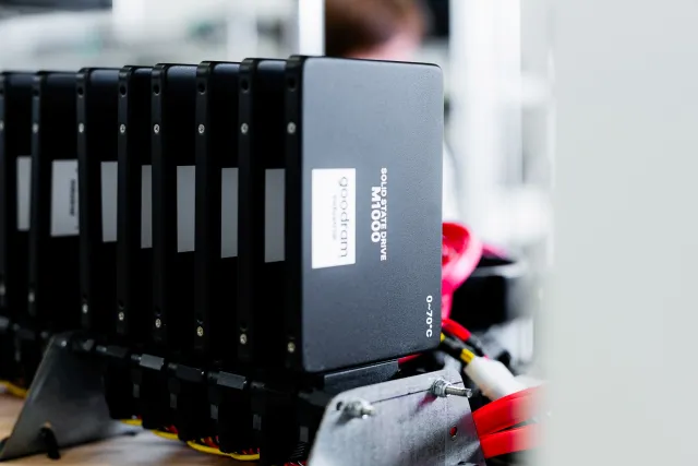
For SSDs, the objective is similar—remove early-life defects—but the method must respect the NAND endurance budget. After controller initialization and firmware integrity checks, the validation flow completes two complete write-and-read cycles across the entire Logical Block Addressing space. For a 1 TB drive, this corresponds to approximately 2 TB of data written during production screening.
Testing is managed in a customized Linux environment that watches SMART attributes and accumulation of Developed Bad Blocks. This makes it possible to observe interface stability, protocol anomalies, transfer errors, and potential PCIe or SATA marginalities while limiting avoidable NAND wear.

Environmental Qualification: From Board Interconnects to Application Platforms
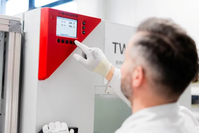
Production electrical screening answers whether a device works under stress. Environmental qualification asks whether the package, solder joints, PCB materials, and nearby components survive temperature and humidity variation. A Binder MKTF 240 climatic chamber supports this role, offering a temperature range from −70°C to +180°C together with humidity control. Relevant procedures can reference the IEC 60068 series, including IEC 60068-2-14 and IEC 60068-2-30, as well as MIL-STD-810.
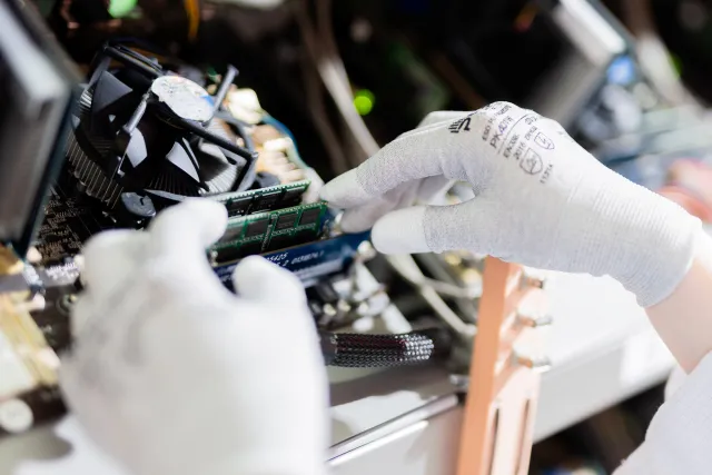
For embedded manufacturers, a practical feature is validation on customer-supplied hardware. Testing memory in the target platform exposes compatibility issues that generic motherboards may miss, especially when BIOS settings, power delivery, controller scheduling, or mechanical constraints affect operation.
BOM Stability and Firmware Tuning: Avoiding Silent Configuration Drift
In real-time or deterministic systems, changing a controller revision or memory die process can create compatibility and timing issues even if the replacement part appears electrically similar. Goodram Industrial Solutions addresses this through a fixed Bill of Materials (BOM freeze), intended to keep component configuration consistent across production batches. Firmware optimization is also available: for example, SSD behavior can be tuned to favor lower write latency rather than maximum sequential throughput when the workload demands responsive small writes.
Comparison Table: What Each Validation Layer Is Designed to Reveal
| Validation layer | Core engineering question | Industrial risk reduced | Evidence expected in supplier review |
|---|---|---|---|
| DRAM thermal burn-in | Can retention or timing defects be forced out at elevated temperature? | Intermittent data errors and module instability during long operation. | Full-load condition at 80°C and stress duration between 30 and 180 minutes. |
| Host compatibility farm | Will the module negotiate correctly with the memory controllers used in deployed systems? | Boot failures, reduced capacity, or ECC behavior differences across hosts. | Use of more than 400 diagnostic platforms and more than 400 computer platforms based on Intel and AMD architectures. |
| SSD whole-LBA screening | Can the drive write and read its full address space without exhausting unnecessary endurance? | Latent block failure, firmware/interface errors, and premature SSD replacement. | Two complete write-and-read cycles; on a 1 TB drive, approximately 2 TB written. |
| Environmental chamber qualification | Do interconnects and materials survive temperature and humidity cycling? | Solder-joint degradation, PCB stress, and intermittent failures in enclosures or cold/hot plants. | Binder MKTF 240 range −70°C to +180°C with standards such as IEC 60068 series, IEC 60068-2-14, IEC 60068-2-30, and MIL-STD-810. |
| Configuration control | Will future batches remain electrically and firmware compatible? | Recertification burden and unpredictable behavior after component substitution. | Goodram Industrial Solutions BOM freeze and application-oriented firmware optimization. |
Procurement Checklist for Semiconductor and Embedded Teams
- Ask whether the supplier separates DRAM and SSD test algorithms according to failure physics rather than applying one generic screening profile.
- Request evidence of thermal stress, not only room-temperature functional pass/fail data.
- Verify host diversity, including ECC and Registered DIMM use cases when the platform architecture requires them.
- Confirm whether validation can be run on the integrator’s own motherboard or target enclosure rather than a reference board.
- Check for BOM stability commitments and change-notification practices before placing multi-year orders.
- Review firmware tunability when the workload is dominated by small, latency-sensitive writes rather than large sequential transfers.
Common Misconceptions About Industrial Memory and Storage Testing
- “A basic electrical test is enough.” Standard functional checks may miss defects that appear after thermal, timing, protocol, or endurance stress.
- “Longer test time is always better.” Excessive screening can raise cost and, for NAND-based SSDs, may wear cells before shipment.
- “All DRAM suppliers are interchangeable.” Host controllers, die generations, ECC behavior, and batch consistency can create meaningful differences in embedded platforms.
- “Firmware settings never affect system timing.” SSD parameter selection can shift latency and throughput priorities, changing deterministic behavior in industrial applications.
- “Supply-chain geography is unrelated to component quality.” R&D, labs, and manufacturing located together can shorten investigation loops when marginalities appear.
Data Points Cited in This Analysis
- DRAM thermal burn-in: 80°C, measured at component surfaces, for between 30 and 180 minutes depending on procedure.
- Test infrastructure: more than 400 diagnostic platforms and more than 400 computer platforms based on Intel and AMD architectures.
- SSD screening: two complete write-and-read cycles across the LBA space; for 1 TB, approximately 2 TB written.
- Environmental chamber: Binder MKTF 240, with −70°C to +180°C range and humidity control.
- Standards referenced: IEC 60068 series, including IEC 60068-2-14 and IEC 60068-2-30, plus MIL-STD-810.
- Company context: Goodram S.A., established 1991, serving over 40 markets and manufacturing in the European Union.
- Event context: electronica 2026 in Munich; In 2026, supply-chain resilience is a recurring industrial electronics theme.
Supply-Chain and Company Context for Industrial Buyers
Goodram S.A. describes itself as a Polish manufacturer of DRAM memory modules and SSDs, based in Łaziska Górne since 1991. The company states that it is the only manufacturer of those items in the European Union and that its products are delivered to over 40 markets. For semiconductor buyers, the relevance of this operating footprint is not symbolic; it reflects integration of design, test, and production at one site in Poland. That co-location can simplify technical communication among R&D, quality assurance, and manufacturing teams when a compatibility issue or BOM question needs follow-up. The Goodram Industrial and Goodram Enterprise portfolios target industrial, embedded, server, data center, and AI workloads.
Industry participation is also cited through the Polish Technology Platform for Photonics, abbreviated as PPTF, and the Polish Chamber of Commerce for Electronics and Telecommunications, abbreviated as KIGEiT. Goodram Industrial is noted as being present at electronica 2026 in Munich, an event that has become a reference point for discussions on European technological sovereignty, resilient sourcing, and industrial electronics supply-chain strategy.

Action Advice for Design, Procurement, and Integration Teams
- Map memory failures to system outcomes before selecting parts: identify the line stoppage, data loss, or maintenance penalty that a DRAM or SSD defect would cause.
- Require test methodology as part of the qualification package. The relevant questions are: DRAM burn-in condition, SSD endurance consumption, host coverage, environmental chamber capability, and address-to-die mapping.
- Run supplier samples on the intended target platform, especially if the system uses ECC, Registered DIMM configurations, or mixed PCIe and SATA interfaces.
- Document acceptable BOM and firmware states. If the platform depends on deterministic latency, specify which performance profile is approved and how future revisions will be communicated.
- Align sourcing decisions with risk windows. Near electronica 2026, many teams revisit supplier geography, batch traceability, and environmental qualification records before approving long-life industrial designs.
FAQ for Semiconductor and Embedded Integrators
Why do thermal and environmental tests matter after electrical screening?
Electrical screening may detect immediate opens, shorts, or obvious functional faults. Thermal acceleration, such as full-load operation at 80°C, can expose weaker retention and marginal timing. Environmental cycling with a Binder MKTF 240 chamber can expose interconnect and material stress that does not show on a bench setup.
Why should SSD validation limit excessive write cycles?
SSDs have a finite endurance budget, often described in terms of bytes written. The validation method described here uses two complete write-and-read cycles, which equals approximately 2 TB for a 1 TB drive, while monitoring SMART and Developed Bad Blocks. This balances defect detection against avoidable wear.
What does BOM stability prevent?
A silent substitution of a controller, DRAM die, or firmware version may change timing, compatibility, or deterministic behavior. Goodram Industrial Solutions offers a fixed Bill of Materials to help maintain consistent component configuration across production batches.
Is manufacturing location a semiconductor quality factor?
Location alone does not guarantee quality, but when R&D, test laboratories, and manufacturing are in the same facility, investigation loops can be shorter. In this case study, that integration is described at Łaziska Górne, Poland, and is relevant to European OEMs and integrators evaluating supply-chain resilience in 2026.
Final Reading for Industrial Computing Designers
Memory and storage qualification becomes actionable when engineers connect each test layer to a failure mechanism: DRAM retention and timing defects, SSD block and protocol errors, interconnect degradation under humidity and temperature cycling, or silent configuration drift across batches. The Goodram case, with its focus on 80°C stress, more than 400 diagnostic platforms, whole-LBA validation, environmental chambers, and BOM freeze options, is best understood as a reliability engineering workflow rather than a marketing description. For Electronicseng readers in Semiconductors, the takeaway is to ask suppliers for test evidence that matches the physics of the device and the operating reality of the target system.