
Semiconductors Brief on Electronicseng: Rapidus, IBM and Chitose City Test Japan's 2 nm Comeback Plan
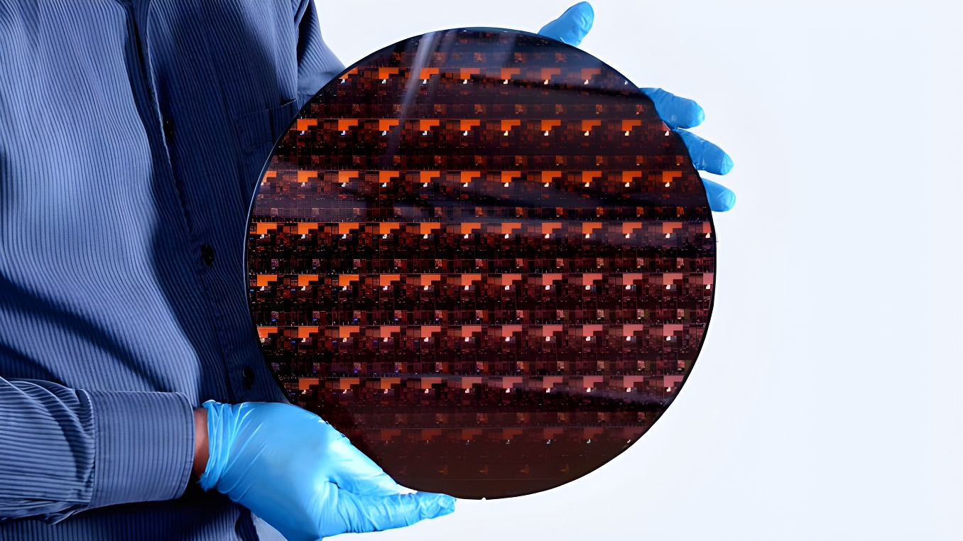
For semiconductor teams tracking advanced-node supply options, the Rapidus program in Chitose City, Hokkaido, Japan, should be read as a stress test of how national policy, licensed process technology and late-stage industrial coordination combine to bring a 2 nm logic node from project plan to product supply. IBM's deepened collaboration and its presence in Hokkaido are presented not as a cosmetic relocation, but as part of the support structure around Japan's attempt to revive domestic cutting-edge chip manufacturing. The headline target is 2027 mass production, while the nearer operational question is whether a newly built wafer facility, pilot equipment and IBM-derived technology transfer can be aligned quickly enough to de-risk the first production window.
Rapidus sits at the center of this effort. The company is backed by the Japanese government and by an investor group that includes Toyota, Denso, Sony Group, SoftBank, NTT, Kioxia, NEC and Mitsubishi UFJ Bank. Its stated direction is to use advanced process technology as a way to restore Japan's competitiveness and to narrow the distance to leading manufacturers such as TSMC, Samsung Electronics and Intel.
In recent years, Japanese policy attention has intensified around advanced logic fabrication. From the perspective of Tokyo, the stakes are not limited to commercial electronics supply. The source material frames 2 nm manufacturing as linked to economic competitiveness, industrial security and supply-chain autonomy, which explains why a domestic advanced-node venture attracts state-level financial support and cross-industry backing.
What the Chitose City project signals for advanced logic sourcing
The Rapidus fab is not positioned as a conservative incremental climb through mature process steps. Instead, the company is attempting to enter the advanced logic market directly at the 2 nm node. That choice compresses the usual sequence of process maturity, yield learning and customer qualification. It creates a fast-track possibility, but it also raises execution risk because the project must simultaneously prove a fab build, a toolset ramp, a transferred design-to-manufacturing flow and commercial readiness.
IBM's role is described as foundational rather than peripheral. Rapidus has taken a license to IBM-developed 2 nm manufacturing technology, and the two parties continue joint development. The announced IBM presence in Chitose City is therefore interpreted as support for technology transfer, engineering capability building, talent development and production preparation. For electronics engineers, that matters because a licensed frontier node is not a standalone file handoff; it becomes usable only when local process control, design enablement, packaging interfaces, test infrastructure and manufacturing operations mature together.
The factory itself is moving through the early hardware phase. The site in Chitose City is under construction, and pilot-line equipment installation related to trial production has been initiated. The plan is to expand the scale of process verification within the next few months, which creates a practical set of checkpoints ahead of the 2027 production objective. The sequence from pilot line to mass production is where much of the project's credibility will be judged.
Project anchors: evidence points used in this brief
The following are the concrete facts reported in the source material and used as a tracking checklist for semiconductor planners. They are presented as verified reference points rather than expanded market estimates.
- Company: Rapidus.
- Technology partner: IBM.
- Target node: 2 nm.
- Target production year: 2027.
- Fab location: Chitose City, Hokkaido, Japan.
- State support: Japanese government financial backing, with policy interest expressed from Tokyo.
- Investor group: Toyota, Denso, Sony Group, SoftBank, NTT, Kioxia, NEC and Mitsubishi UFJ Bank.
- Competitive reference set: TSMC, Samsung Electronics and Intel.
- Current phase: wafer fab construction, start of pilot-line equipment installation and planned expansion of process verification within the next few months.
- Strategic background: Japan has been out of the leading position in advanced logic manufacturing for decades.
Comparison table: how the 2027 Rapidus plan differs from a conventional foundry ramp
| Dimension | Position reflected in the source material | Engineering or procurement implication |
|---|---|---|
| Technology entry point | Direct move to 2 nm | Compresses the learning curve but leaves less room for gradual qualification failures. |
| Manufacturing location | Chitose City in Hokkaido, Japan | Creates a new domestic site rather than relying on an established advanced-node cluster. |
| Technology source | IBM licensing and continued joint development | Project progress depends on transferring frontier know-how into local manufacturing operations. |
| Timeline marker | 2027 mass production goal | Buyers should focus on intermediate milestones such as pilot-line equipment status and process verification. |
| Current operational stage | Construction plus pilot-line equipment installation, with wider process verification planned within the next few months | The short-term signal is validation scale-up, not shipping volume. |
| Capital and policy backing | Japanese government and a broad Japanese industrial investor group | Supports continuity but does not automatically remove technical or commercial risk. |
| Strategic aim | Rebuild Japan's position in advanced logic and reduce dependence on existing leading foundry centers | If successful, it could add another qualifying source for advanced-node chips. |
| Risk characterization | High risk | Projects entering directly at a leading node face tighter margin for schedule slippage, integration defects and customer qualification delays. |
Common misconceptions
- Misconception 1: IBM is taking over manufacturing. The source describes IBM as a licensed technology partner and collaborator whose presence supports Rapidus. The factory effort remains centered on Rapidus in Chitose City.
- Misconception 2: A 2 nm node announcement is equivalent to 2 nm supply. The reported goal is 2027 mass production. Before that, the project is still moving through construction, pilot-line equipment installation and expanded process verification.
- Misconception 3: Japanese government funding removes commercial execution risk. State support and industrial investor backing improve resource depth, but the plan is still described as high risk because Rapidus is not entering through a stepwise mature-node path.
- Misconception 4: This is only a domestic Japan story. The source material frames the potential outcome as a supply-chain change: a new advanced manufacturing source could reduce reliance on the existing major wafer foundry centers.
FAQ
Why is IBM relevant to the Rapidus 2 nm timeline?
Rapidus obtained access to IBM-developed 2 nm manufacturing technology, and the two organizations are continuing joint development. IBM's Chitose City presence is treated as an accelerator for technology transfer, production preparation and local engineering capability.
What is Rapidus trying to prove between now and 2027?
It needs to demonstrate that a newly built site can move from pilot-line equipment installation to broader process verification within the next few months, and then to mass production readiness by the stated 2027 target.
Which companies are named as the industrial support base?
Toyota, Denso, Sony Group, SoftBank, NTT, Kioxia, NEC and Mitsubishi UFJ Bank are listed as corporate backers of Rapidus, alongside the Japanese government.
Why is the 2 nm entry considered unusual?
Most process development paths build capability from less advanced nodes toward leading-edge nodes. Rapidus is attempting a direct 2 nm entry, which could shorten the route to relevance but increases the penalty for missed milestones or weak qualification.
What would success mean for the global semiconductor landscape?
If 2 nm production is reached as planned, Japan would return to the leading edge after decades away from the top tier of advanced logic manufacturing. The source also frames this as adding a new potential source of advanced fabrication capacity.
Action recommendations for semiconductor professionals
- Track validation milestones, not headlines. The near-term technical marker is whether expanded process verification within the next few months proceeds from pilot-line equipment installation into reproducible process learning.
- Separate funding certainty from node readiness. Japanese government support and the investor group provide strategic continuity, but 2 nm manufacturing still requires equipment, yield, test, supply-chain and customer qualification alignment.
- Monitor the IBM-to-Rapidus transfer path. For design teams and procurement groups, the practical question is whether licensed 2 nm technology becomes a fully supported local manufacturing platform, not whether an agreement exists.
- Evaluate the project as a possible future second source. If the Chitose City fab reaches qualification, it could diversify dependence on TSMC, Samsung Electronics and Intel, but sourcing decisions should wait for verified process and production status.
- Keep Japan's policy objective in view. The source connects the 2 nm plan to industrial security and supply-chain autonomy, which means the project may influence national semiconductor planning beyond the immediate wafer output.
The practical reading is that Japan's 2 nm ambition is being assembled from multiple parts at once: state backing, a licensed technology base, an industrial consortium, a new Hokkaido fab site and a compressed validation schedule. The 2027 target gives the project a visible deadline, but the decisive progress will be measured through the next operational steps in Chitose City.