
Electronicseng Semiconductors: Infineon’s €1.1bn 300mm GaN Power Chip Expansion Explained for Engineers
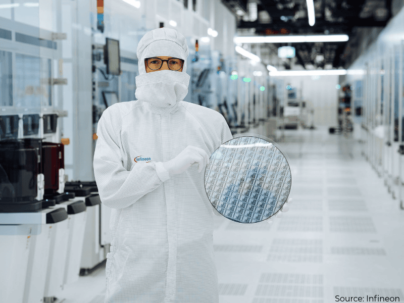
Around €1.1 billion is being committed by Infineon Technologies to its Villach site in Austria, for what the company describes as the first high-volume GaN power-chip plant worldwide built on 300mm wafers. Output is expected by the end of 2027, with investment running through 2034.
The relevance for power-electronics teams is direct: it links a larger European manufacturing position to GaN scaling for AI data centers, electric vehicles, industrial systems, energy systems and robotics. For Electronicseng readers, the question is not only where the fab sits, but whether wafer-scale output can help GaN move beyond niche power conversion use.
Manufacturing step: reusing cleanrooms while scaling 300mm GaN
Instead of building from a blank site, the expansion is designed to use existing cleanroom infrastructure at Villach, coupling upgraded production capacity with established operations to reduce the cost of scaling.
The first 300mm GaN wafers were processed by Infineon in 2024, demonstrating a path that could deliver approximately 2.3 times as many chips per wafer as conventional 200mm manufacturing. The company is extending that capability toward high-volume production and matching capacity ramp-up with demand.
Relative to conventional silicon-based power devices, GaN devices are described as offering faster switching, lower power losses and reduced heat generation, which supports smaller and more efficient power conversion systems.
“This substantial investment shows our clear commitment to strengthening the European semiconductor ecosystem and Europe’s technological sovereignty. By establishing high-volume manufacturing on 300-millimeter wafers, we will be the first company in the world to bring gallium nitride power electronics into volume production,” said Jochen Hanebeck, CEO of Infineon Technologies AG.
Policy backdrop: European Chips Act aid with one approval still open
Support for the project includes €319 million in state aid cleared by the European Commission under the European Chips Act. A formal funding decision from Austria’s Federal Ministry for Economic Affairs, Energy and Tourism has not yet arrived.
The investment is intended to strengthen Europe’s semiconductor manufacturing base while encouraging links among industry, universities, research organizations and smaller technology companies.
Villach is already a major hub for Infineon’s power semiconductor research and manufacturing. The site employs around 4,800 people, and Austria-wide staffing is approximately 5,800 employees. The new facility is also expected to tie GaN manufacturing closer to regional power electronics R&D work.
Checklist: what semiconductor teams should note
- Timeline: 300mm GaN wafer processing in 2024; volume manufacturing expected by the end of 2027; investment horizon through 2034.
- Output scale: 300mm offers approximately 2.3 times as many chips per wafer than 200mm.
- Device benefit: GaN provides faster switching, lower power losses and reduced heat generation versus silicon-based power devices.
- Funding state: €319 million approved by the European Commission under the European Chips Act, while the Federal Ministry decision remains pending.
- Site relevance: Villach in Austria hosts around 4,800 people, and Austria-wide employment is approximately 5,800 employees.
Comparison table: 200mm baseline, 300mm GaN and silicon device contrast
| Reference point | Original baseline | Infineon Villach direction |
|---|---|---|
| Wafer size | Conventional 200mm manufacturing | 300mm wafers for GaN power semiconductors |
| Per-wafer chips | 200mm baseline | Approximately 2.3 times as many chips |
| Production milestone | First 300mm GaN wafer processing in 2024 | Manufacturing by the end of 2027, investment through 2034 |
| Power device behavior | Silicon-based power devices | Faster switching, lower power losses and reduced heat generation |
| Market pull | GaN moving beyond niche applications | AI data centers, electric vehicles, industrial systems, energy systems and robotics |
| Policy support | European Chips Act | €319 million approved by the European Commission; Austrian ministry approval pending |
Data citation: Yole Group’s GaN market outlook
Yole Group’s Power GaN 2026 report is the cited demand marker: the global GaN power semiconductor market could reach approximately $3.5 billion by 2031, with annual growth of around 35% between 2025 and 2031.
Infineon frames 300mm as a way to support greater production scale as GaN shifts from niche uses toward mainstream power electronics.
Common misconceptions to avoid
- 2024 does not mean volume output. The 300mm GaN wafers processed in 2024 are a process milestone; the stated production target is by the end of 2027.
- State aid is partially approved. The European Commission has approved €319 million under the European Chips Act, but the Federal Ministry for Economic Affairs, Energy and Tourism approval remains pending.
- 300mm is not a standalone performance claim. It relates to wafer-level output and manufacturing scale, while the stated device advantages are faster switching, lower power losses and reduced heat generation versus silicon-based power devices.
FAQ: decision points for engineers and supply-chain readers
Does the €1.1bn expansion mean GaN supply changes now?
No. Infineon processed its first 300mm GaN wafers in 2024, but the plan targets high-volume manufacturing by the end of 2027, with investment continuing through 2034.
Why is 300mm important for GaN power chips?
The company says the format can produce approximately 2.3 times as many chips per wafer as conventional 200mm manufacturing, and the Villach facility uses existing cleanroom infrastructure to reduce expansion cost.
Which European policy facts matter here?
The project receives €319 million in state aid approved by the European Commission under the European Chips Act. Approval from Austria’s Federal Ministry for Economic Affairs, Energy and Tourism is still pending.
What device-level advantages are stated?
Compared with conventional silicon-based power devices, GaN devices are presented as enabling faster switching, lower power losses and reduced heat generation, which can support smaller and more efficient power conversion systems.
Action recommendations
- Anchor roadmaps to the disclosed milestones: in 2024 processing evidence, by the end of 2027 production, and through 2034 investment.
- Map possible GaN adoption in AI data centers, electric vehicles, industrial systems, energy systems and robotics, then compare device benefits against silicon-based power devices.
- Watch the Villach and Austria manufacturing node, including around 4,800 people at the site and approximately 5,800 employees across Austria.
- Track the policy condition: €319 million approved by the European Commission under the European Chips Act, but Austrian ministry approval remains pending.
- Use the cited market context cautiously: Yole Group’s Power GaN 2026 report points to approximately $3.5 billion by 2031 and around 35% annual growth between 2025 and 2031.
The practical takeaway is that this is an Infineon Technologies move to connect 300-millimeter wafers, European Chips Act support, and Europe-based GaN manufacturing at Villach. Its importance for Electronicseng readers lies in whether the stated 2.3 times per-wafer output potential and GaN device advantages can help the industry scale power electronics for AI infrastructure and electrification.