
Electronicseng Semiconductors: a VCSEL, two ICs, and package notes from a multimode 850 nm SFP teardown
By Rachel Williams
Viewed as a semiconductor assembly rather than as a generic network accessory, a small pluggable optical transceiver contains a transmit emitter, a receive detector, supporting silicon, and a latch-and-case mechanism. This note examines one such part: an 850 nm multimode SFP module, set against the single-mode teardown published Last month.
For today, the specimen is still an SFP, not a higher-speed SFP+, and it came bundled with a media converter; the converter is retained as a spare for possible future lightning-strike galvanic isolation. The internal parts are modest in number: a VCSEL transmitter, a spectrally tuned receiver, two ICs, and a small mechanical assembly.
Wavelength labels and the fiber-type boundary
Before looking at the module, the wavelength names need a reminder from the earlier SFP tutorial. The labels below are not full spectral windows; all are center frequencies:
- 850 nm (“multimode”)
- 1300 nm (“multimode”) / 1310 nm (“single-mode”)
- 1550 nm (“single-mode”)
multimode and single-mode are two technologies, and they are not interchangeable, although some modules can work with both associated cable material types. The prior single-mode part may have used Fabry-Perot or distributed-feedback (DFB) construction; confident visual separation is not possible, and knowledgeable reader insights are welcome. The present 850 nm multimode optical module uses neither.
Comparison table: core size, emitter, and trade-off
| Attribute | multimode path | single-mode path |
|---|---|---|
| Typical labels | 850 nm; 1300 nm in the multimode tutorial grouping | 1310 nm; 1550 nm |
| Fiber core | 50 to 62.5 microns | 8 to 10 microns |
| Optic shape | Larger core lets multiple light signals follow different paths. | Tiny core lets one ray pass through without edge bounce. |
| Emitter family | uses lower-cost LEDs or vertical-cavity surface-emitting lasers (VCSELs) | Focused lasers |
| Historical trade-off | lower implementation cost with shorter usable transmission distance | longer usable distance, historically higher cost |
| Cost note | lower cost was a reason to accept shorter reach. | cost disadvantage has more recently decreased because non-proprietary, widely compatible modules are available. |
Data citation: the wavelength labels, core dimensions, and emitter description come from the earlier tutorial quoted in this teardown; the single-mode compatibility note and the cost-compatibility observation also come from that same reference material.
Emitter choice and the sub-Gbit ceiling
The excerpt uses lower-cost LEDs or vertical-cavity surface-emitting lasers (VCSELs) remains strictly accurate, though it is now half-obsolete. Near-infrared LEDs did appear in early sub-Gbit 850 nm SFP modules.
A helpful reference note states: their maximum rate of about 622 Mb/s meant that they could not support 1 Gb/s or higher transmission.
That ceiling supports the expectation that a modern 850 nm module will use a VCSEL transmitter, not an LED, and that the detector will be a spectrally tuned variant of the earlier 1310-nm receiver rather than the same part.
Red glow from a near-infrared source
The spectrum association was checked without instruments: the module was inserted into an SFP cage on a multi-port switch in a dark room, and a small red glow was visible from the transmit connector.
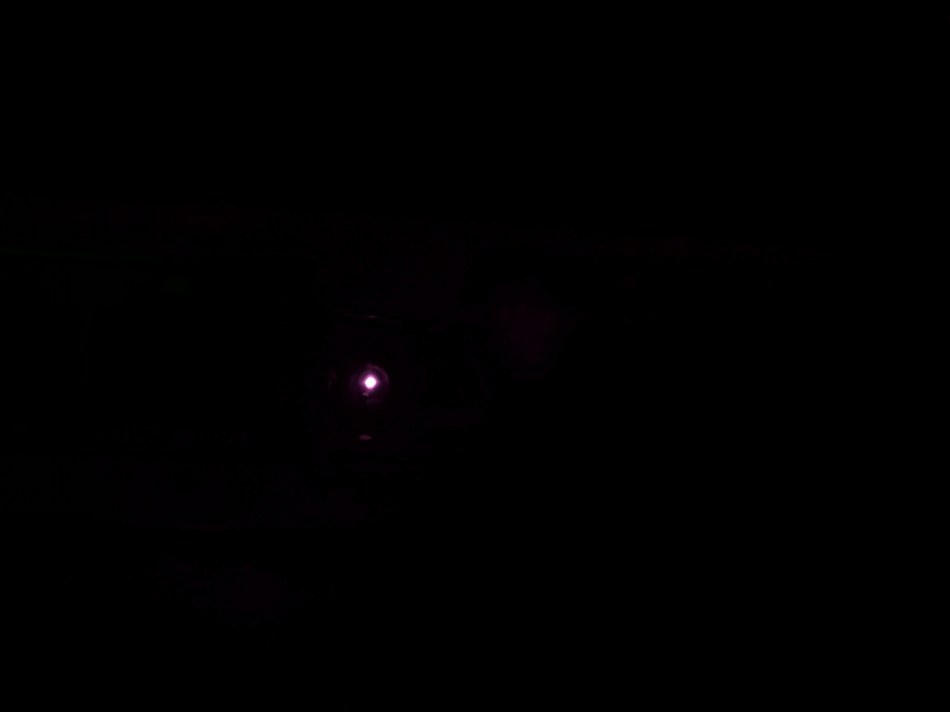
Visible perception normally ends around 750 nm, corresponding to a ~400 THz frequency. The transmit source is listed at 850 nm, or ~3.5 THz, so the eye should not see the center wavelength. The observed dim red glow implies that the transmitter output distribution, which has a bell curve(-ish) profile, still contains some energy at the visible wavelength end of its overall distribution.
External package views, in sequence
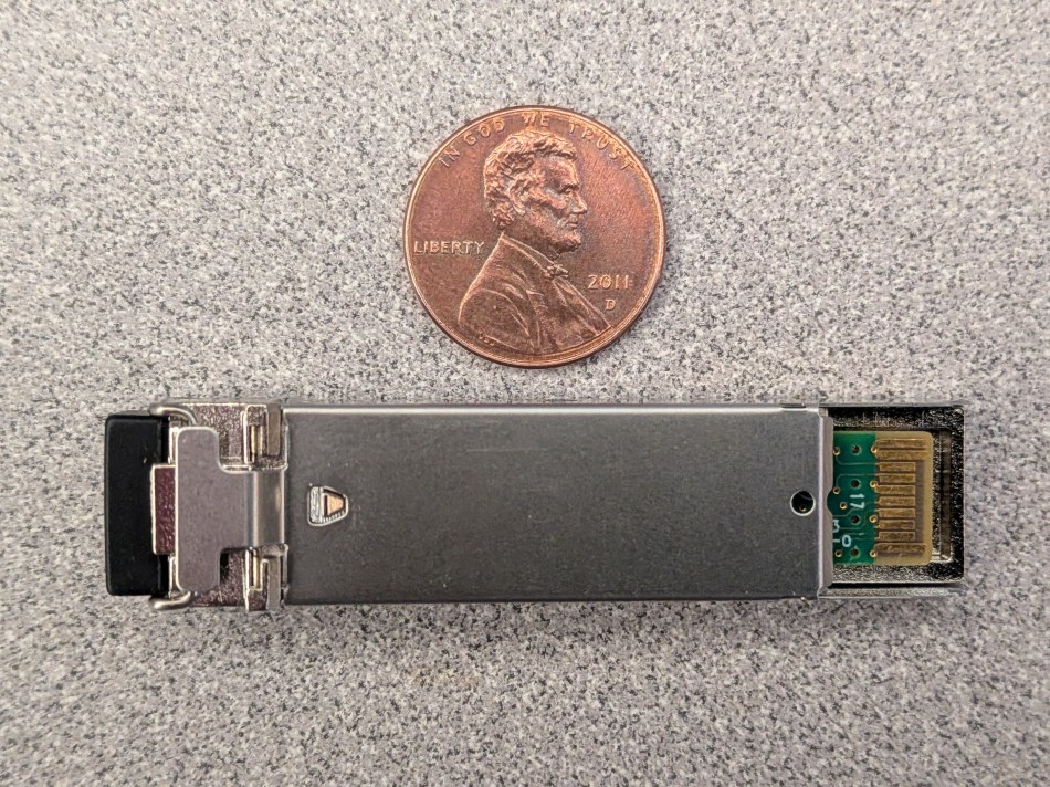
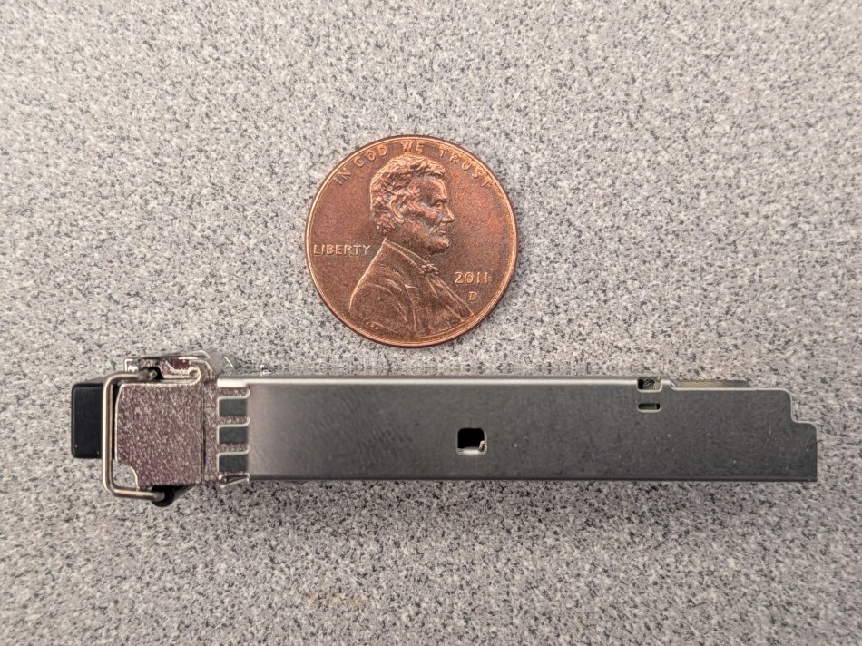
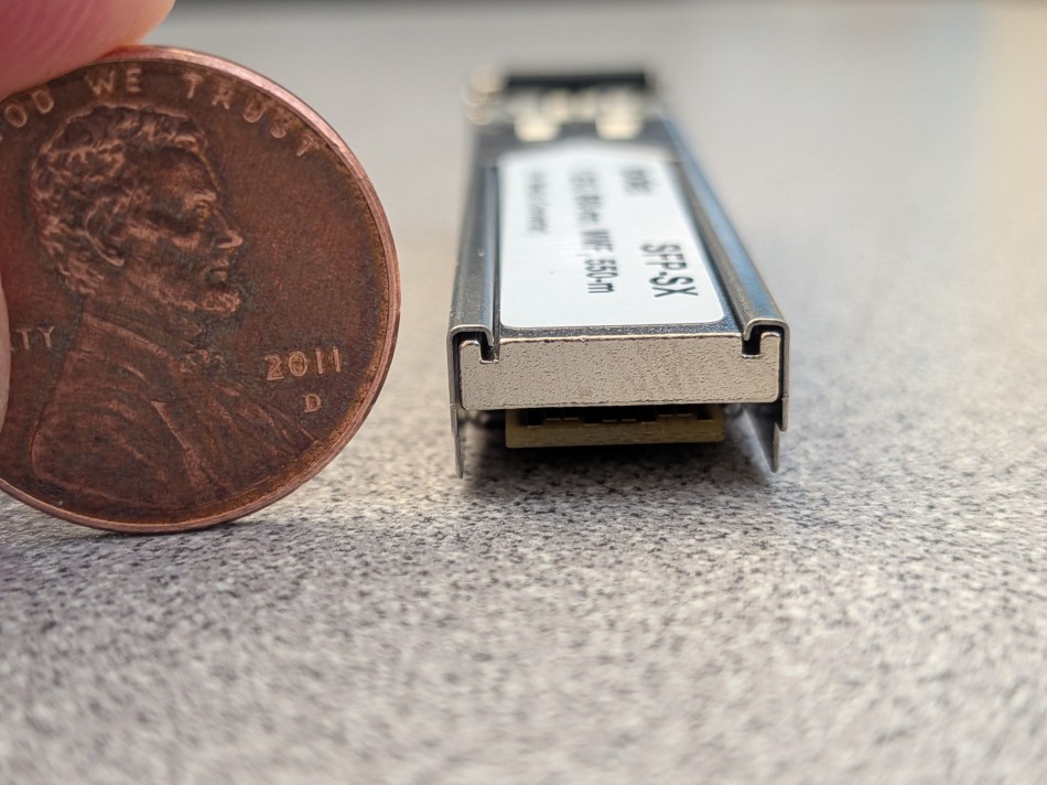
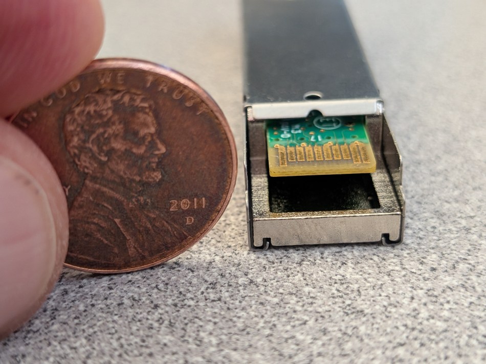
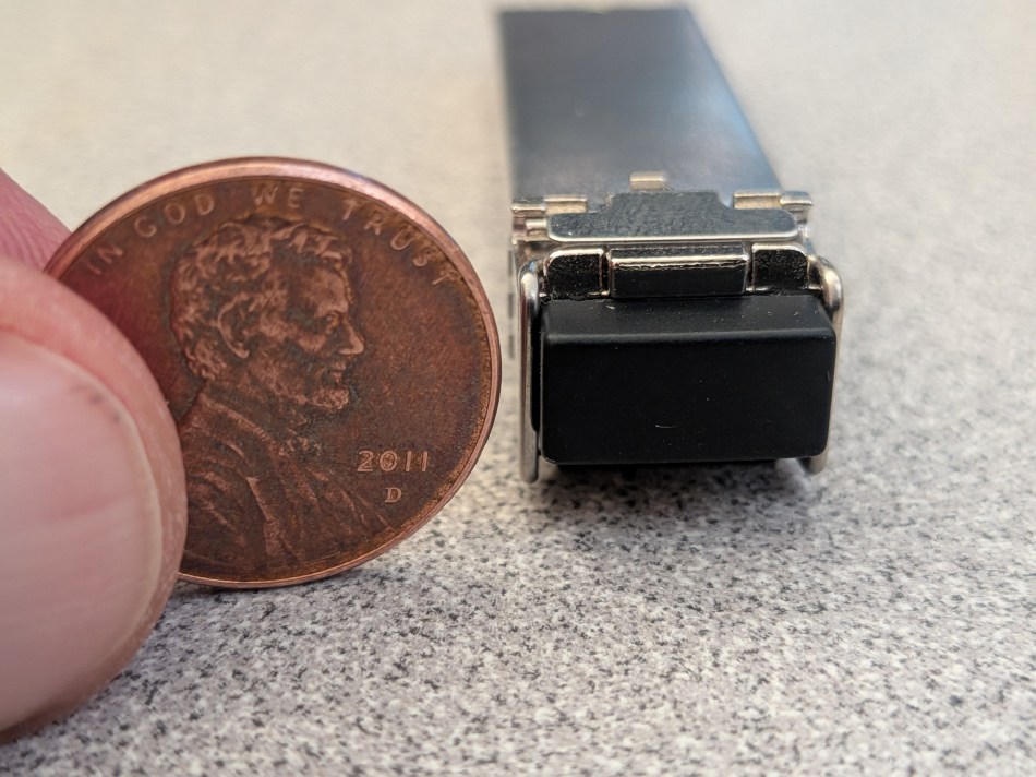
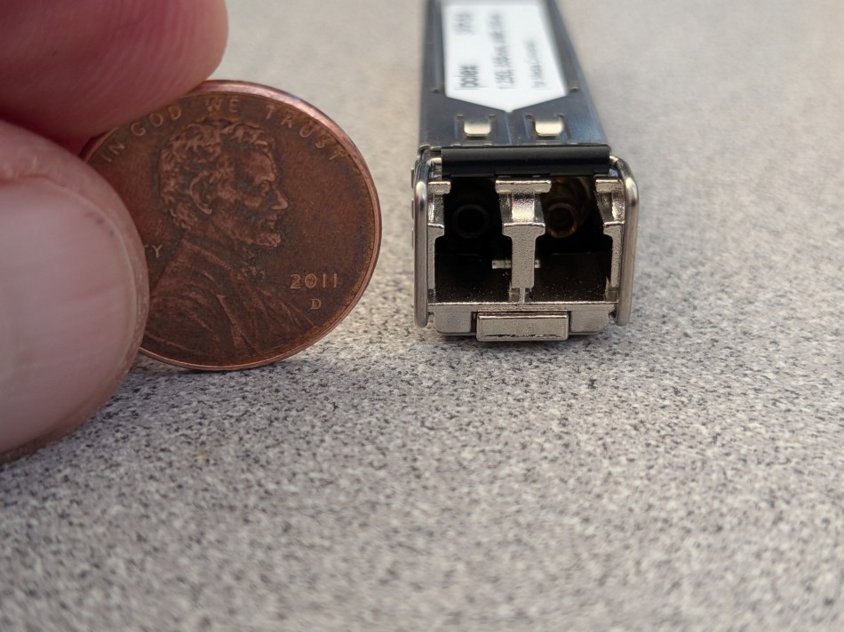
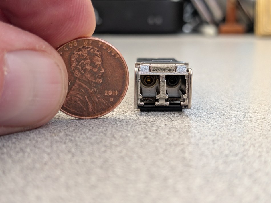
The usual scale reference is included: a 0.75″ (19.1 mm) diameter U.S. penny.
Upper surface.
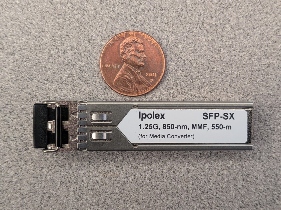
A close view of the embossed transmit and receive direction arrows, also seen in the Last month teardown and generally found on optical modules.
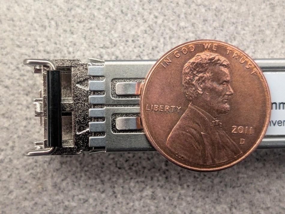
right side, meaning the right when viewed with the module oriented for insertion in a switch or similar SFP port.
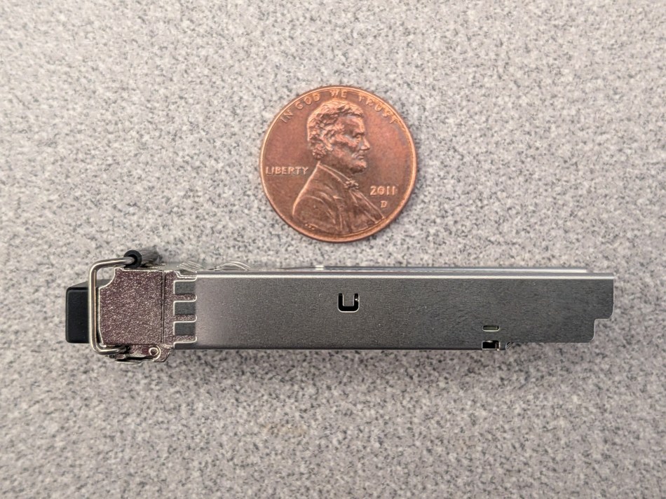
Lower surface, including the retractable retaining pin.
Left side.
Electrical connector end, normal orientation.
Electrical connector end, inverted orientation.
Optical connector end with dust cap, normal orientation.
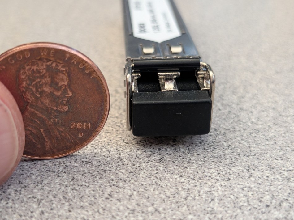
Optical connector end with dust cap, inverted orientation.
Optical connector end after cap removal, normal orientation.
Optical connector end after cap removal, inverted orientation.
Opening the housing
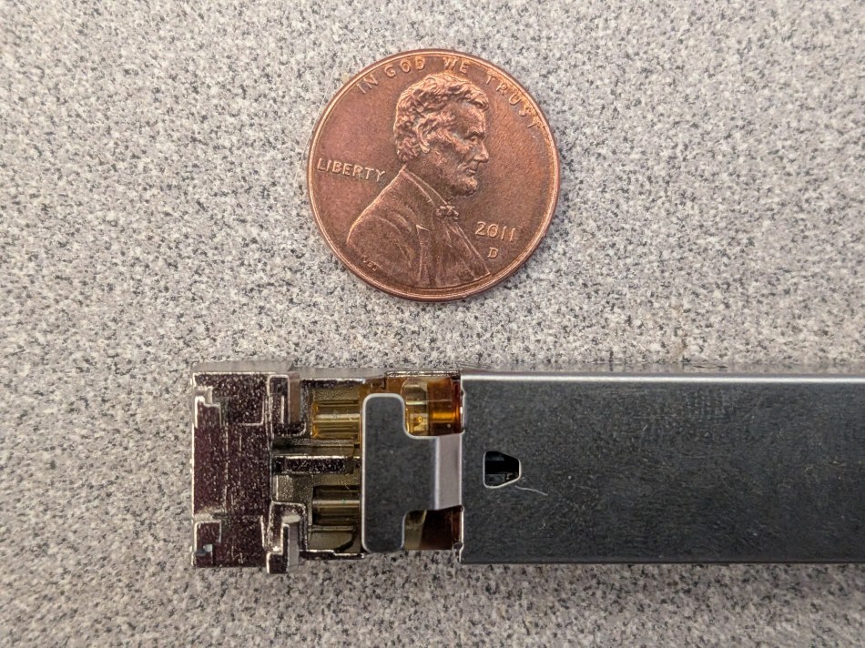
The outer and inner enclosure pieces are held by side tabs. As in the previous module, there are two tabs, one on each side; only the left side tab was initially depressed. Bending the tab opens the path to the interior.
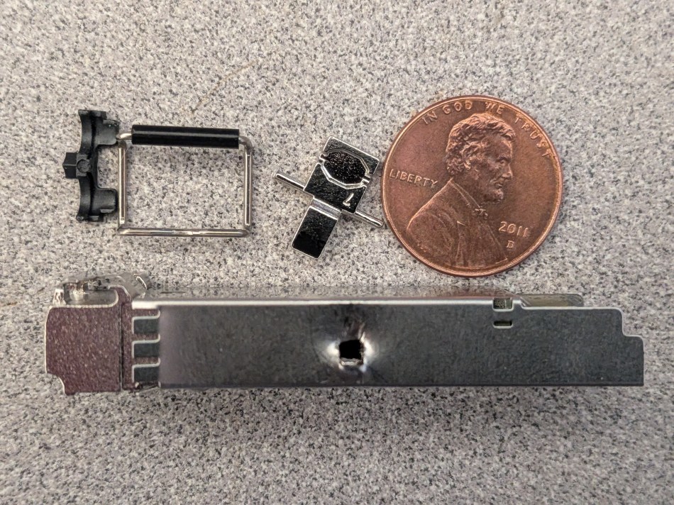
The hinge and associated pieces separated with the enclosure halves, as they did in the Last month teardown.
With the halves removed, the inner assembly is exposed.
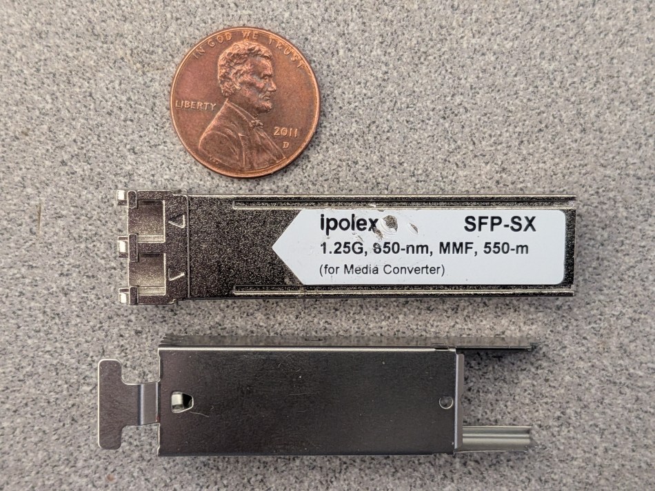
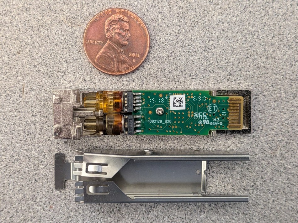
One screw retains the PCB to the surrounding metal assembly.
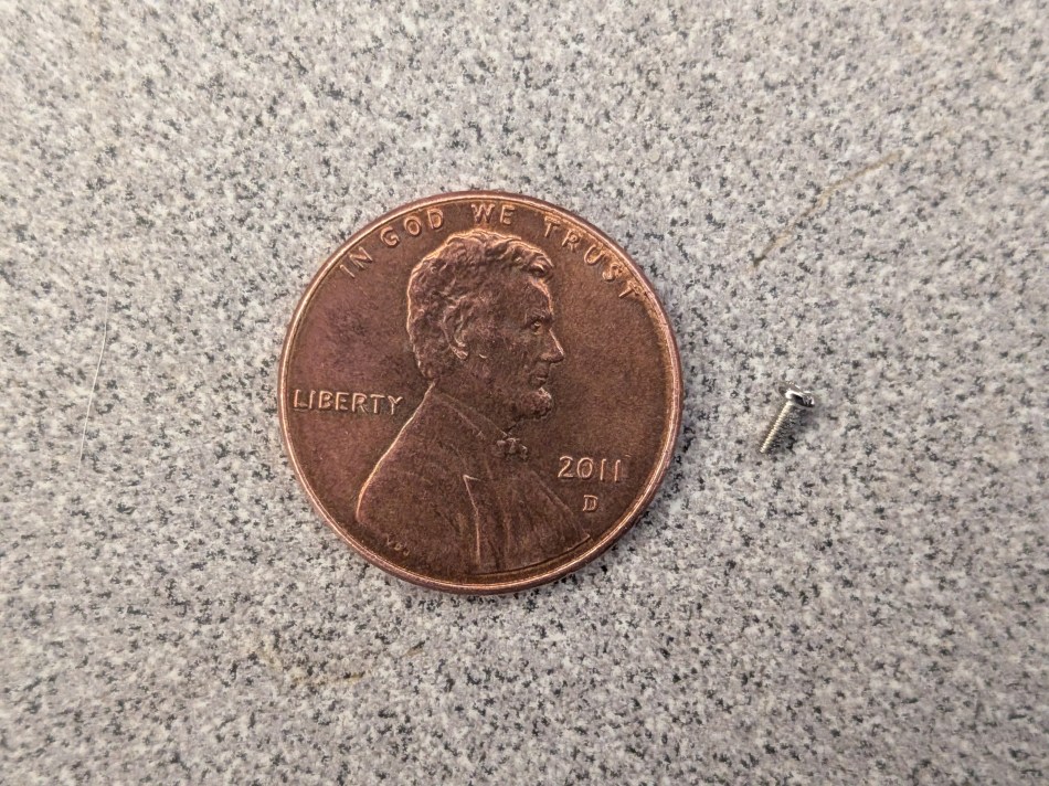
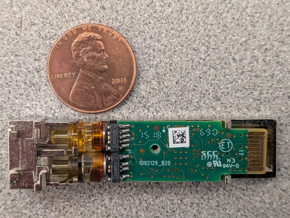
Once the screw is out, the board is free.
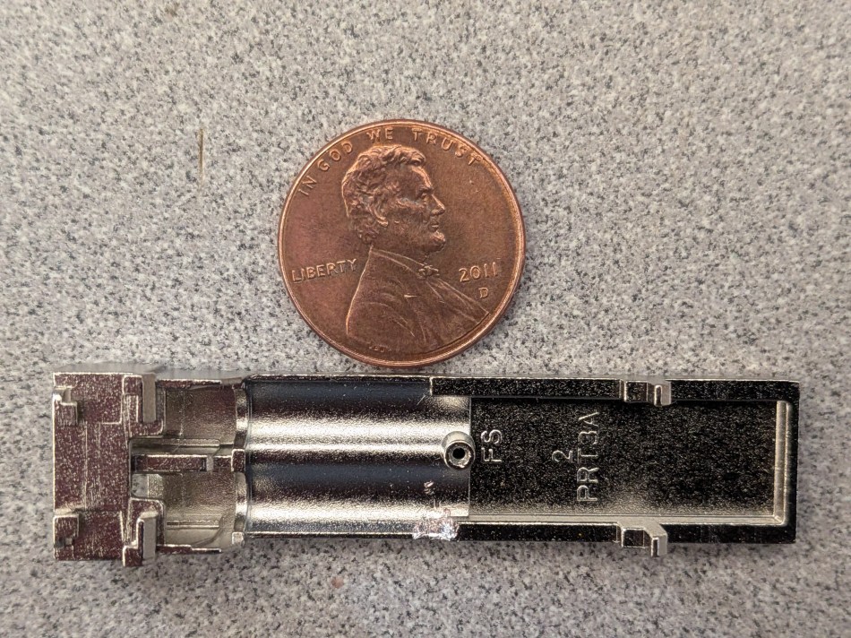
Board-side optics and receiver/transmitter placement
Bottom side.
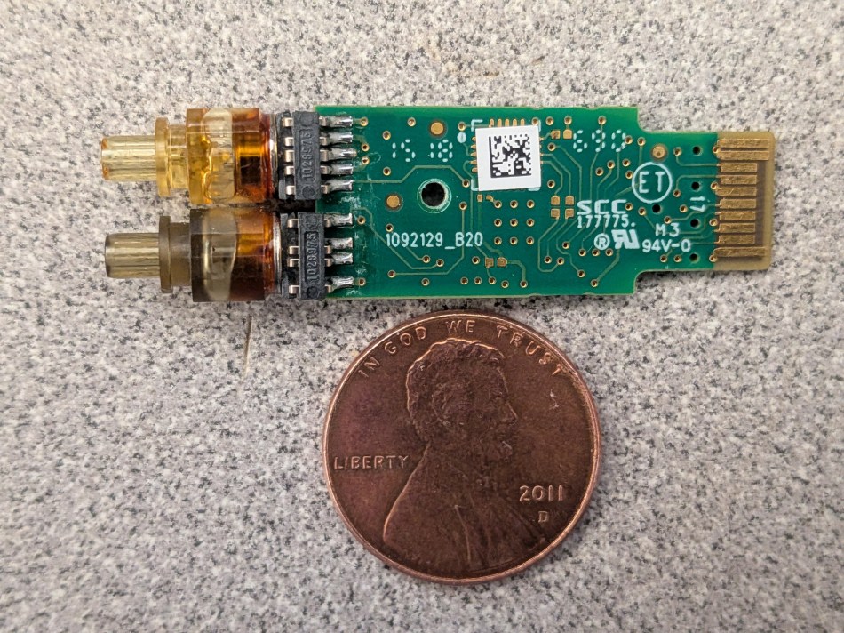
The optical receiver module is on the left edge of the top side, visually similar to the receiver in the prior single-mode SFP, but tuned for a different incoming signal wavelength. Below it sits the 850 nm VCSEL-based transmitter, which looks very different from the 1310 nm laser transmitter shown in the next comparison image.
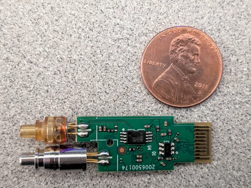
PCB topside.
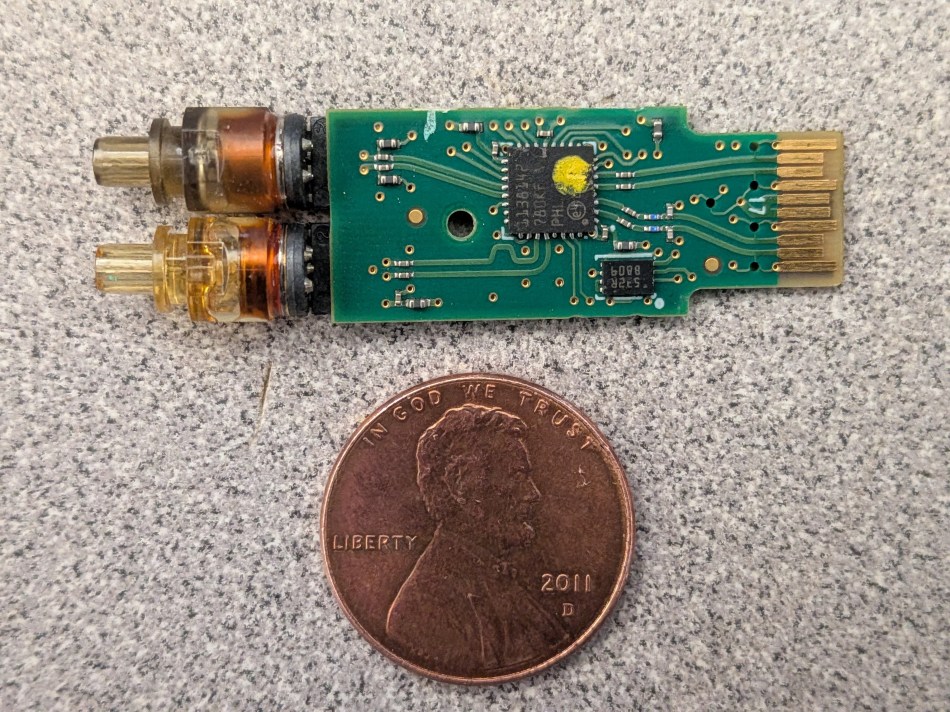
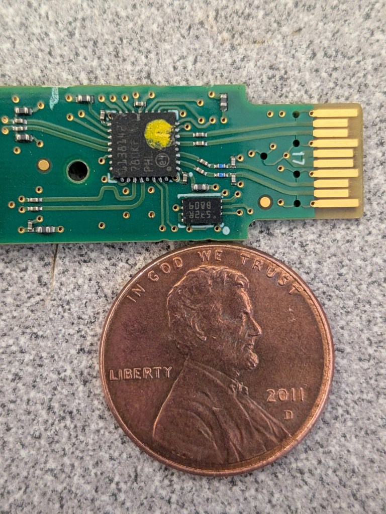
On the topside the placement is reversed: transmitter at the upper left and receiver below it. The next image highlights the two ICs.
Markings, IC identity, and EEPROM inference
The larger of the two ICs has this four-line topside mark:
1138142
780KF VJ; the second character might instead be the letter O
PHL, followed by a three-digit code partly hidden by yellow paint; in an online photo the code is 141, but this unit does not appear to show 141, and the first character looks like B
e4, circled like a logo, with an obscured two-character code ES
A Google search on the phrase 1138142 IC suggests that STMicroelectronics is the supplier but does not reveal anything about the chip's function. Reader insights are welcome.
The smaller IC is marked:
532R
B809; the third character here may instead be the letter O
As with the single-mode module, the smaller part is assumed to be an EEPROM storing data such as the module serial number, vendor name, compatibility codes, and calibration data.
The SFP interface and the LC, or Lucent Connector, ends of the PCB are visually identical to those in the Last month module, so the redundant photos are omitted; see Last month teardown images for equivalent views.
Common misconceptions this teardown helps avoid
- Believing 850 nm cannot produce any visible spot. The center wavelength is beyond normal vision, but the output distribution can still reach visible wavelengths.
- Assuming every 850 nm part uses an LED. Modern 850 nm modules point to a VCSEL transmitter because the LED era was limited below the speed now required.
- Confusing multimode and single-mode as interchangeable fiber families. They are two technologies, even though some modules may work with both associated cable material types.
Teardown and inspection checklist
- Confirm the wavelength grouping first: 850 nm is multimode, while 1310 nm and 1550 nm are single-mode.
- Check the fiber core assumption: 50 to 62.5 microns for multimode, 8 to 10 microns for single-mode.
- For 850 nm parts above the LED era, expect a VCSEL transmitter rather than a low-rate LED.
- Before disassembly, note the direction arrows, retractable retaining pin, and the fact that two tabs hold the enclosure.
- After opening, look for loose hinge pieces before the PCB moves.
- Do not lose One screw if separating the PCB from the metal assembly.
- Record the four-line topside mark details for larger IC: 1138142, 780KF, PHL with hidden three-digit code, and e4 with two-character code ES.
- Assume the smaller 532R / B809 part is an EEPROM, as inferred from the single-mode module comparison.
FAQ
Why discuss a red dot for an infrared module?
Because 850 nm is a center frequency, not a sharp cutoff. The module was checked in a dark room, and the dim red glow indicates visible-end energy in the transmit distribution.
Why can LED-based 850 nm parts not serve higher speeds?
The reference limit is direct: their maximum rate of about 622 Mb/s meant that they could not support 1 Gb/s or higher transmission.
What did the IC markings prove?
They did not fully prove function. The larger part is linked to STMicroelectronics by a Google search on 1138142 IC, but the chip role remains unconfirmed; the smaller part is an EEPROM inference.
Action recommendations
- For optical-link design review, compare wavelength, core size, and emitter type together; do not judge cost or distance from the 850 nm label alone.
- For module sourcing, note that non-proprietary, widely compatible modules are available and can change the historical single-mode versus multimode cost comparison.
- For lab inspection, document direction arrows, retaining-pin action, dust-cap condition, and tab locations before opening, then observe the two tabs and hinge pieces as they separate.
- For teardown documentation, preserve ambiguous markings in context: note where O may be a letter, where the three-digit code is obscured, and where 141 may not be visible on the unit.