
Can Z2RAM Redraw the Memory Map for AI Chips? A Semiconductors Deep Dive from Electronicseng
Memory, not compute, is increasingly the binding constraint on accelerator design. That premise is what makes a two-transistor cell concept from a US startup worth a close read by engineers sizing on-die SRAM, evaluating HBM stacks, or planning multi-chip inference topologies. Below, we unpack the device physics, the claimed density uplift, the integration route, and the supply-side reality that sets the actual adoption clock.
Who Is Behind the Technology
The technology is branded Z2RAM and comes from Nagare Labs, a US startup co-founded by Georgia Tech researchers Suman Datta and Shimeng Yu. Their background is years of work on emerging memories, including ferroelectric and resistive RAM devices.
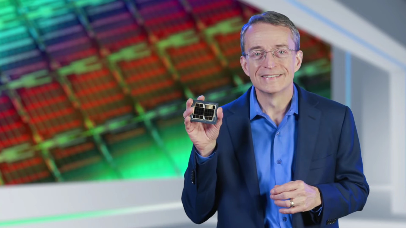
Playground Global, the investment firm in which Pat Gelsinger takes part, led the company's USD 5 million seed round. The thesis he has articulated is that Z2RAM could combine the strengths of SRAM, DRAM and flash into one memory class that is simultaneously dense, fast and scalable.
His framing of the problem: over the past three decades, mainstream commercially deployed memory has not fundamentally changed. SRAM, DRAM and NAND flash still form the storage base of modern computing hardware, while AI compute demand exposes the limits of that arrangement.
The Device-Level Change: Where the Charge Lives
The core novelty is a redesigned way of holding charge in the cell.
| Cell type | Structure | Charge storage | Read behavior | Density / cost trade-off |
| Conventional DRAM | 1T1C: one transistor plus one capacitor | Dedicated capacitor | Destructive — charge is consumed and must be rewritten; periodic refresh required | High density, but refresh and peripheral overhead |
| Conventional SRAM | Typically six transistors per cell | Cross-coupled latch | Non-destructive, very fast; no periodic refresh | Large cell area, high cost per bit, hard to scale to high capacity |
| Z2RAM (concept) | Two transistors per cell, no discrete DRAM-style capacitor | Gate capacitance of the second transistor | Claimed non-destructive read, so no rewrite step after read | Aimed at bridging SRAM speed with far higher area density |
Suman Datta's explanation of the payoff is that eliminating the post-read rewrite should cut access latency and improve overall memory efficiency, while the two-transistor cell attacks the area problem that makes SRAM expensive.
Claimed Density and Bandwidth: What It Buys an AI Processor
Nagare Labs projects that the first-generation Z2RAM can reach more than five times the storage density per unit area of conventional SRAM. Worked through: where a given area of SRAM yields 64 MB capacity, the same area in Z2RAM should theoretically lift capacity to roughly 320 MB while retaining bandwidth close to SRAM levels.
That matters because today's accelerators are caught between two imperfect options:
- HBM-heavy designs. AI accelerators lean on HBM for enormous memory bandwidth, but HBM requires complex stacked packaging, drives manufacturing cost up, and constrains power and package area.
- SRAM-heavy designs. Some inference-focused processors place large amounts of on-die SRAM to minimize latency to external memory, but limited SRAM density forces a hard split of silicon area between capacity and compute.
Nvidia Groq 3 LPU is the clearest illustration: it adopts large amounts of SRAM as on-chip storage resource, with per-chip SRAM capacity of about 500 MB. Under Nagare Labs' own assumption, a five times density figure would let the same area hold several multiples of that data, which could reduce the number of processors a large inference system needs and ease inter-chip data movement pressure.
Integration Route: Oxide Semiconductors and 3D Hybrid Bonding
Two process choices define the pitch. First, Z2RAM is built on oxide semiconductor materials and is intended to be integrated directly above the compute logic die via 3D hybrid bonding. In principle that frees the design from the classic separated memory-plus-processor architecture, shortening data travel distance by stacking a high-density memory layer close to the logic.
The mental model is partly AMD's 3D V-Cache, which stacks additional SRAM cache on a processor — except Z2RAM targets higher storage density than a cache stack.
Second, the manufacturing plan borrows the vertical stacking logic of NAND flash, building multiple memory tiers layer by layer. Rather than depending on the complex high-density packaging that HBM and LPDDR require, the company hopes oxide semiconductors plus back-end processing can deliver comparatively simple multi-layer fabrication. If it works, the cost of large on-die storage pools comes down.
Engineering Risks: Standards, Reliability, Clock Speed
Reality check: this is very early-stage R&D. The USD 5 million seed round has just closed, present results are laboratory prototypes, and mature tape-out has not happened.
Nagare Labs is looking for fab partners able to support development manufacturing, to move the work from a university cleanroom into larger-scale production validation. Stated timeline: working Z2RAM memory chip samples within the next four years, commercial shipments targeted within the next ten years.
Three risk clusters dominate:
- Interface standardization. Connecting Z2RAM to a processor or accelerator via 3D hybrid bonding requires an interface, and no unified industry standard exists for a memory of this kind. Georgia Tech researchers note that without a mature standard the company may have to develop its own interface technology, adding design and commercialization complexity.
- Material reliability. Oxide semiconductors bring advantages in thermal stability and radiation tolerance, but atomic vacancies and similar microscopic defects can appear in the material. These can shift transistor threshold voltage; even a small voltage change can push a cell into a data error.
- Qualification burden. For a memory product, reliability outranks peak lab performance. Long-term data retention, endurance across read/write cycles, temperature variation and manufacturing consistency all have to be proven before commercial entry.
Nagare Labs' own co-founders acknowledge the graveyard: many memory startups have tried to challenge conventional DRAM and flash and failed. Strong lab metrics do not equal passing the semiconductor industry's quality gates or entering existing compute supply chains.
Supply Context: Not a Near-Term Fix for the Memory Squeeze
Current global memory tightness is driven by surging AI datacenter demand, plus Samsung, SK Hynix and Micron shifting more capacity toward HBM and server memory products. Z2RAM will not relieve that shortage — even engineering samples in four years sit far from volume production.
Its significance, if it ships, is architectural rather than volumetric. Pat Gelsinger's view is that a successful Z2RAM could offer a different answer on density, speed and power than today's HBM-centric approach, letting AI processors hold larger high-speed storage pools on-chip, reducing dependence on external memory bandwidth, and giving next-generation accelerators a new design option.
Source attribution for the underlying reporting: Ars Technica +2.
Selection Checklist: How to Track Z2RAM as a Design Variable
- Treat published density multiples as projections until a silicon datasheet with measured retention and endurance exists.
- Model area savings against your own compute-to-capacity ratio before assuming fewer chips per inference cluster.
- Ask any vendor about interconnect: a proprietary 3D bonded interface means you own the standardization risk.
- Demand threshold-voltage distribution data, not means; oxide vacancy defects show up in the tail.
- Keep HBM and LPDDR roadmaps as your primary supply plan through the next four years at minimum.
- Watch for a confirmed fab partner — production validation, not papers, is the real milestone.
Common Misreadings
- "It replaces DRAM." The concept targets an SRAM-class role with higher density, not a bulk DRAM substitution.
- "It eases the memory shortage." It does not add near-term conventional memory supply.
- "Two transistors means cheaper by default." Cost depends on stacking yield, bonding throughput and qualification rates.
- "Five times is a guaranteed product spec." It is a first-generation estimate tied to unspecified process conditions.
FAQ
Q: What exactly is Z2RAM?
A: A two-transistor memory cell concept from Nagare Labs that stores charge on the second transistor's gate capacitance instead of a separate capacitor, aiming for SRAM-like speed with far higher area density.
Q: Who invested?
A: Playground Global led a USD 5 million seed round; Pat Gelsinger participates in that firm.
Q: When could samples exist?
A: The company's stated plan is working samples within the next four years and commercial shipments within the next ten years.
Q: How does it differ from 3D V-Cache?
A: Both use stacked die integration near logic, but 3D V-Cache stacks conventional SRAM, while Z2RAM proposes a different cell with, per the startup's projection, more than five times the density of SRAM.
Q: Should procurement plans change now?
A: No. Plan on the HBM, LPDDR and DDR supply picture; treat Z2RAM as an architectural option to re-evaluate after first engineering samples.
Actionable Takeaways
- Architecture teams: run an internal study quantifying how a 5x on-die storage density change would reshape your compute-to-memory ratio.
- Supply-chain owners: keep capacity commitments with Samsung, SK Hynix and Micron aligned to the HBM and server-memory tightness cycle, and diarize a reassessment at the four-year sample window.
- Reliability engineers: build an evaluation template now covering data retention, read/write endurance, threshold-voltage spread across temperature, and multi-layer bonding yield.
- Analysts: score emerging-memory startups on fab partnership and qualification evidence rather than lab performance claims.
From SRAM to DRAM to NAND flash, the storage hierarchy has been settled for a long run. Z2RAM is an attempt to break the long-standing density-versus-speed trade-off between those tiers. Right now it remains a laboratory-stage concept; whether it matures into a competitive commercial product is a question for time and manufacturing process to answer, not for the funding announcement.
Prepared by the Electronicseng editorial team — Semiconductor desk. For questions about this coverage or corrections, contact info@electronicseng.com.
Written by Rachel Williams, Electronics & Engineering.