
MemFlation Explained: How Macronix Is Repositioning NOR, SLC NAND and eMMC for the AI Tier Shift
By Rachel Williams, Electronics & Engineering — Electronicseng Semiconductors desk
Design and sourcing teams that froze their memory budget eighteen months ago are reopening the spreadsheet. The trigger is not the familiar inventory swing but a deliberate reallocation of wafer starts and capital: Samsung, SK Hynix and Micron have pushed resources toward high-bandwidth memory (HBM) and advanced server DRAM to feed AI accelerators, and the strain has landed on parts that rarely headline analyst calls — NOR flash, SLC NAND and eMMC. For an engineer or procurement lead, the working question has moved from “will prices rise” to “which tier of the memory hierarchy is still designable inside my cost, power and supply envelope.” What follows unpacks the structural reading offered by Macronix, traces it to concrete node, voltage and packaging decisions, and converts it into qualification actions you can take this quarter.

The Repricing Is Structural, Not Cyclical
Martin Lin, director of marketing at Macronix International, put the case to EE Times Taiwan in terms that are explicitly architectural rather than volumetric. In his words, “the entire memory architecture is changing.” NOR flash is appearing in far more AI servers than in conventional ones, system architects are looking for a tier that offers more capacity and better cost efficiency than HBM, and key-value (KV) cache has become a first-order determinant of inference performance. Memory, on this reading, stops behaving like a passive storage component and starts behaving like a variable in the performance, cost and topology equation.
The supporting figures are unusually stark. Data referenced by the company shows the market passing $20 billion in 2025 and potentially approaching $70 billion in 2026, with growth coming less from shipment volume than from price itself — the condition Macronix calls “memory inflation,” or “MemFlation.” Cumulative price movement over the past year is described as sixfold, and the company expects further upward movement followed by an elevated plateau through the third and fourth quarters of 2026.
Scope matters when you budget by category. Macronix expects the combined market for NOR flash, SLC NAND and low-capacity eMMC (≤32GB) to reach around $24 billion in 2026. Within that, NOR faces relatively moderate increases because capacity was committed earlier, while SLC NAND and eMMC remain under heavier supply pressure. Independent market trackers describe the same asymmetry: SLC NAND contract prices have been forecast to rise by well over 100% in the second half of 2026 versus the first half, eMMC pricing has been reported as roughly doubling within a single quarter, and several suppliers are discontinuing low-density parts, forcing industrial and automotive customers to redesign toward higher-endurance cells.
Capacity is not the quick fix it appears to be on a roadmap slide. Even where a line upgrade is approved today, equipment installation, process qualification and yield ramp-up can take two to three years, if not longer. Macronix has lifted capital expenditure for 2026 to NT$37.8 billion to expand 12-inch wafer capacity aimed at 3D NOR, NAND, eMMC and related products — a response that relieves supply only on a multi-year horizon. With mature-process capacity still being crowded out by AI demand, automotive programs should expect allocation limits and pricing strain to become clearly visible from 2027.
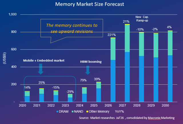 Supply-side reallocation, not demand recovery, is what is driving the price curve.
Inside the AI Rack: NOR Content Multiplies
The most concrete board-level signal is flash count per rack. A conventional server typically required only about three to five flash devices to cover boot, firmware, system control and security functions. An AI server carries many more, because baseboard management controllers (BMCs), network switches, retimers and smart control boards each need their own code storage and their own root of trust. Lin quantified the jump: “The previous-generation rack had around 600 to 800 devices. The latest generation now has more than 1,000”.
Two consequences deserve engineering attention. First, a boot tier that used to be a rounding error in the bill of materials now interacts directly with unit price, so density-per-device and multi-purpose firmware partitions become cost levers rather than afterthoughts. Second, the boot and firmware path inherits datacenter reliability expectations — retention across thermal cycling, power-loss robustness, secure boot and rollback protection — which shrinks the pool of qualified parts and lengthens second-source approval cycles.
Past the HBM Ceiling: Candidates for a New Tier
If the rack-level flash count is a change in “quantity,” the more consequential shift is hierarchical. AI training and inference depend on HBM because it is the only tier that matches GPU bandwidth appetite; Lin is blunt that “only HBM is fast enough” today. Yet adding capacity by stacking more HBM layers raises cost steeply, so the industry is searching for a tier that trades a modest amount of bandwidth for a large amount of gigabytes at better cost efficiency.
High-bandwidth flash (HBF) is the leading candidate. Built on stacked 3D NAND and paired with high-speed interfaces and dense, HBM-style packaging, it relocates data that does not need to live in HBM into a higher-capacity, relatively lower-cost NAND tier. The first openly published HBF contribution — 512GB-class stacks with aggregate bandwidth targets in the region of 3 TB/s, announced through the Open Compute Project with SK Hynix participating alongside a NAND partner — indicates the tier is moving from concept toward hardware. Parallel work in AI server architecture pushes enterprise SSDs toward very high input/output per second (IOPS) levels, while low-latency SLC NAND absorbs the random-access traffic GPUs generate, improving accelerator utilization.
Inference is where tiering pays back fastest. Large language models (LLMs) and agentic AI workloads must continuously retain conversation, task and historical information, so KV cache only grows. Describing continuous conversations, Lin noted that if capacity falls short, “you have to discard the earlier information.” The workable pattern is classification by data age, access frequency and latency requirement: the hottest, most latency-sensitive tensors stay in HBM, while bulk context that does not demand sustained high-speed access migrates to flash, SSD and other tiers. At the recent Future Memory and Storage conference (FMS 2026) in the United States, Macronix presented its dual-tier SSD architecture as one answer for KV-cache offloading.
| Tier | What it should hold | Engineering role | Signal to monitor |
|---|---|---|---|
| HBM | Hot weights, activations, latency-critical KV | Only tier meeting GPU bandwidth appetite | Capacity booked far out; every added layer raises system cost |
| HBF (emerging) | Cold weights, long context, model archives | NAND density with stacked, high-speed packaging | Standardization stage; single-vendor risk for now |
| Low-latency SLC NAND | Boot images, write buffers, random GPU accesses | Deterministic latency and high endurance | Heaviest squeeze; allocation and long lead times |
| 3D NAND / dual-tier SSD | Offloaded KV cache, training and inference datasets | Capacity per dollar and per watt | Repricing as AI data centers and enterprise SSDs absorb supply |
| NOR flash | Boot, firmware, BMC, secure control paths | Execute-in-place and root of trust | Moderate price steps, but per-rack device count rising sharply |
| eMMC ≤32GB | Legacy embedded system storage | Cost-effective capacity in mature designs | Low densities discontinued; redesign or respecification needed |
Data Movement, Not Flops, Sets the Ceiling
As accelerators keep gaining compute, the binding constraint shifts from raw speed to whether data arrives in time. Lin's formulation: “The GPU is already fast enough, but now , memory is actually too slow.” Each repeated transfer among CPU, GPU, HBM, DRAM and storage consumes bandwidth and adds latency and power, so raising processor speed alone stops translating into end-to-end performance.
That is why the industry is revisiting memory-centric designs and processing-in-memory (PIM) architectures: bringing computation closer to the array, or letting memory perform simple operations before outputting results, cuts round trips. The idea is not new — Macronix Chairman and CEO Miin Wu proposed “Memory-centric AI” as early as 2019 — but the growth of models, datasets and inference workloads has put it back in front of both industry and academia. Lin's expectation for the next stage is that gains will come as much from memory architecture as from faster GPUs, pushing development toward questions of where data sits, how it moves and when it is processed.
Node, Voltage and Layer Count: What to Lock In
Product strategy is following the architecture. Alongside higher supply of high-density NOR for AI servers, Macronix is widening its NAND and eMMC portfolios and advancing 3D NAND to cover more capacities and applications. It currently has 48-layer and 96-layer 3D NAND products in mass production while developing higher layer counts. NOR is moving toward higher density, lower power and greater reliability, with process technology progressing from 55nm to 42nm and 3D NOR under development; its high-density NOR is already deployed in AI servers, and the company is extending into high-reliability automotive, communications, medical and aerospace markets. To address power requirements in AI, industrial and embedded systems, low-voltage flash is progressing from 3V and 1.8V toward 1.2V — a detail that matters on multi-rail boards where the memory rail has become a heat and efficiency line item.
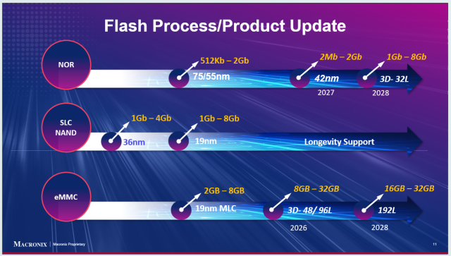 The three flash lines are converging on the same targets: density, capacity and reliability per watt.
| Line | Roadmap direction | Nodes and milestones | Design implication |
|---|---|---|---|
| NOR flash | Higher density, lower power, greater reliability | 55nm to 42nm; 42nm in 2027; 3D-32-layer in 2028 | Consolidate several small boot parts into one larger device |
| SLC NAND | Long-term supply support | Low-latency role in AI random access | Retain as the deterministic tier for OS boot and write buffers |
| eMMC | Higher capacity and density | 3D-48 and 96 layers to 192 layers | Respecify legacy ≤32GB slots early, before second sources vanish |
| 3D NAND | Broader capacity coverage | 48-layer and 96-layer in production, higher stacks in development | Feeds HBF and dual-tier SSD concepts rather than consumer parts |
Common Misconceptions
- “Niche memory tightness ends with the next capex announcement.” Tools, qualification and yield learning still require two to three years; announced capacity is not near-term supply.
- “MemFlation is just vendor language for a shortage.” It describes something measurable: category revenue growing on price while volumes stay flat.
- “NOR is a commodity part that never decides a BOM.” Rack-level device counts have moved from three to five per server to well over a thousand per rack, and the boot tier is security-critical.
- “HBF competes with HBM.” It is positioned underneath HBM, holding colder data so HBM can stay small and expensive where it is truly needed.
- “Swapping MLC for SLC is a drop-in.” Cell behavior, capacity planning, endurance budget and firmware all change, along with unit cost.
- “A 1.2V part drops into a 3V rail.” Level shifting, supply sequencing and re-qualification are required, so migrate at the next board spin.
Action Advice for Design and Sourcing Teams
- Re-cost the memory block of your BOM against the elevated tier of 2026 pricing, and model the 2027 plateau rather than assuming reversion.
- Freeze a second-source list now and begin pin- and firmware-compatible qualification of alternates in NOR and SLC NAND; qualification cycles are the real bottleneck.
- Consolidate capacity upward: a single higher-density NOR can replace several small boot devices, cutting both cost exposure and board area.
- Design a tiering path into the architecture — identify what can live outside HBM, and evaluate KV-cache offload to flash or dual-tier SSD before the next silicon spin.
- Track node and package milestones (42nm NOR in 2027, 3D-32-layer NOR in 2028, eMMC moving from 3D-48 and 96 layers to 192 layers) and align product launches to them.
- Put commitments in writing: long-term agreements, capacity reservations and rolling 12-month forecasts are increasingly the only way to protect automotive and industrial volumes.
- Plan power-rail migration toward 1.2V and budget the re-qualification time it implies.
- Watch FMS 2026 and trade-show disclosures for measured endurance, retention and latency data before adopting new tiers.
FAQ
Why would AI servers need more NOR flash if they already use HBM?
HBM serves the accelerator's data appetite, while NOR serves control: boot code, firmware, BMC logic, network silicon and security functions. More controllers and switches per rack mean more code-storage devices per rack, which is why flash consumption per rack rose from roughly 600-800 units to more than 1,000 in the latest generation.
Is low-latency SLC NAND being replaced by newer tiers?
The opposite is closer to the truth. Because GPUs issue large volumes of random accesses, low-latency SLC NAND is being positioned as the deterministic tier that raises GPU utilization, while higher stack-count 3D NAND carries bulk capacity — which is exactly why SLC supply is squeezed hardest.
What does a dual-tier SSD architecture actually change?
It splits data by temperature: latency-sensitive context stays close to compute, while aging KV-cache blocks move to a slower, denser tier. Presented at the Future Memory and Storage conference (FMS 2026), the approach is about total cost per inference token rather than peak bandwidth.
When should automotive buyers expect relief?
Not soon. With mature-process capacity still crowded out, supply constraints and pricing pressure in automotive are expected to become more visible from 2027, and new capacity still needs two to three years to reach qualified, high-yield production.
Does Macronix's capacity spending change the near-term picture?
Only structurally. The NT$37.8 billion 2026 capital plan for 12-inch capacity addresses 3D NOR, NAND and eMMC demand, but qualification and ramp mean its market effect lands well beyond current planning cycles.
Outlook
Lin's expectation heading into 2027 is that tight supply and demand conditions will remain difficult to ease in the short term: new capacity arrives, but process qualification and yield improvement still consume additional time. For the supplier, the balancing act is between AI server demand, mature-flash gaps and next-generation development; for buyers, it is between locking supply now and redesigning to a tier that does not exist in volume yet. Latest nonvolatile memory technologies and application solutions across automotive electronics and edge AI will be on show at electronica 2026, held November 10–13 in Munich, Germany, at Hall C5, Stand 279 — worth pinning to your qualification calendar before the next roadmap review.
