
Electronicseng Semiconductors Analysis: Microchip POL-05-20S-T GaN Point-of-Load Converter for Space Digital Loads
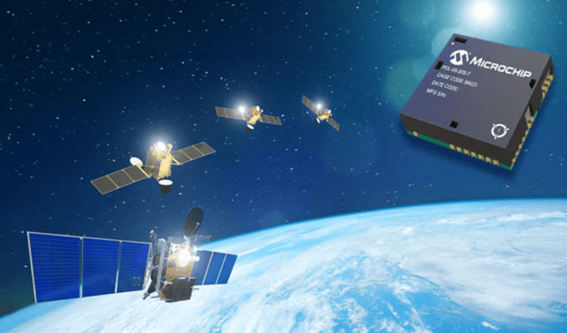
From the Semiconductors desk at Electronicseng, the Microchip POL-05-20S-T can be positioned as a high-current point-of-load building block for onboard digital systems rather than as a general-purpose power module. The source presents it as a GaN POL converter that can supply up to 20 A of continuous current to FPGAs, MCUs, and other processing-intensive digital loads.
That current rating is most useful when paired with the other reported attributes. The device is described as radiation-tolerant, built around GaN power HEMTs, and combining high efficiency with high power density in a compact, lightweight form factor. For engineers designing onboard processing systems, the reported value proposition is therefore the simultaneous treatment of size, power, and energy constraints.
Topology, control behavior, and rail mapping
The converter uses a synchronous buck topology with current-mode control. In the context of POL delivery, that structure is associated with fast transient response and stable operation, two behaviors that matter when digital cores switch between activity states.
The input range is specified as 4.75-V to 13.2-V, and the output is adjustable from 0.7-V to 5-V. Those limits are what allow the part to support multiple power rails and system architectures. A board power tree can place the converter near the load, then assign the adjustable output to a core or peripheral domain without requiring a separate fixed-voltage part for each rail.
Selection checklist for semiconductor and system engineers
- Verify the downstream digital load is one of the stated application classes: FPGA, MCU, or another processing-intensive digital load.
- Use the 20 A continuous current figure as the current-capability reference point from the source.
- Check that upstream distribution can present an input within 4.75-V to 13.2-V.
- Check that the required rail can be generated within the 0.7-V to 5-V adjustable output window.
- Review layout and control-loop assumptions before concluding that fast transient response and stable operation are achieved.
The checklist is intentionally narrow. It follows the published characteristics without expanding them into a mission-level qualification claim.
Radiation, thermal envelope, and device description
Radiation performance is described through two distinct data points. Electrical parameters are specified before and after irradiation up to 50 krad(Si). For single-event effects, characterization extends to a linear energy transfer value of 43 MeV·cm²/mg.
These numbers address different questions. The first relates to electrical parameters after exposure up to the stated dose. The second relates to single-event-effect characterization under the stated LET reference. Treating either number as a complete replacement for mission analysis would extend beyond the source description.
Thermal behavior is presented through the range −55°C to +100°C, across which the converter remains capable of full-load operation. For a POL converter intended to feed 20 A into processing-intensive loads, the thermal range should be read together with efficiency, board heat transfer, and layout, because power density and compact package constraints create an engineering review need rather than a single calculation.
Radiation and thermal reading table
| Reported item | Exact value | Design reading in the source context |
|---|---|---|
| Ionizing dose characterization | 50 krad(Si) | Electrical parameters are specified before and after irradiation up to that dose. |
| Single-event characterization reference | 43 MeV·cm²/mg | SEE characterization extends to that linear energy transfer value. |
| Temperature capability | −55°C to +100°C | Full-load operation is stated across this temperature range. |
| Current capability | 20 A | Continuous current capability for digital loads such as FPGAs and MCUs. |
Package, availability, and sourcing framing
The physical form is reported as a 1.51×1.51×0.45-in. surface-mount package. That data is the mechanical entry point for PCB review: land pattern, assembly, standoff, and clearance considerations all begin with the package outline. The compact nature also reinforces the source description of a small, lightweight form factor aimed at constrained onboard processing systems.
Supply information states that the POL-05-20S-T is now available in production quantities from Microchip Technology. In a component-selection document, that statement should be captured as the availability anchor from the source, while still keeping the device description separate from any unverified procurement status.
Application-oriented comparison
| Design pressure | Source feature | Reported relevance |
|---|---|---|
| Digital current demand | 20 A | Supplies FPGAs, MCUs, and other processing-intensive digital loads. |
| Input rail variation | 4.75-V to 13.2-V | Supports multiple power rails and system architectures. |
| Output voltage flexibility | 0.7-V to 5-V | Adjustable output can be mapped to several digital load domains. |
| Transient stability | Synchronous buck with current-mode control | Provides fast transient response and stable operation. |
| Radiation environment | 50 krad(Si), 43 MeV·cm²/mg | Describes specified dose context and SEE characterization reference. |
| Thermal and mechanical constraint | −55°C to +100°C; 1.51×1.51×0.45-in. | Stated for full-load operation and compact surface-mount integration. |
FAQ: how to interpret the POL-05-20S-T data
What is the role of POL-05-20S-T in a power tree?
The source frames it as a point-of-load converter. That role means it is positioned near digital loads, supplying them with an adjustable low-voltage rail derived from an intermediate input range.
What does the 20 A rating refer to?
It refers to the continuous current capability stated for space digital loads, including FPGAs, MCUs, and other processing-intensive digital loads.
Is the device described as radiation-hardened?
The reported description is radiation-tolerant, with parameters specified up to 50 krad(Si) and SEE characterization to 43 MeV·cm²/mg. Engineers should compare those stated points with mission requirements rather than replacing them with a generic hardening claim.
What package size is specified?
The specified package is 1.51×1.51×0.45-in. and is a surface-mount form factor.
Common misconceptions
- Thinking that the adjustable 0.7-V to 5-V output alone proves system compatibility: the upstream input must still be evaluated against 4.75-V to 13.2-V and the transient behavior of the load.
- Reading the 1.51×1.51×0.45-in. package as evidence that no thermal analysis is needed, even though the source also specifies full-load operation across −55°C to +100°C and a 20 A current role.
- Confusing 50 krad(Si) with 43 MeV·cm²/mg: one is an ionizing dose characterization limit for electrical parameters, the other is a single-event-effect linear energy transfer reference.
Action recommendations for component review
- Place POL-05-20S-T and Microchip Technology into the candidate component record with exact spelling and source-linked availability.
- Record the numeric anchors: 20 A, 4.75-V to 13.2-V, 0.7-V to 5-V, 50 krad(Si), 43 MeV·cm²/mg, −55°C to +100°C, and 1.51×1.51×0.45-in.
- Map the synchronous buck topology and current-mode control into the power-integrity question set for the target board.
- Separate electrical parameter characterization from single-event characterization in the radiation review document.
- Use the surface-mount package data to open mechanical and assembly discussions before treating the compact size as a system-level solution.
For Electronicseng readers following Semiconductors supply and design trends, the Microchip POL-05-20S-T is most clearly described as a compact, GaN-based POL option for high-current digital processing near the load. Its reported specification set gives a concrete basis for early selection, while final system qualification remains a separate design task.