
USFP Connector Economics: How NVIDIA and Cisco Optics Push 400 Gb/s-per-lane AI Factories
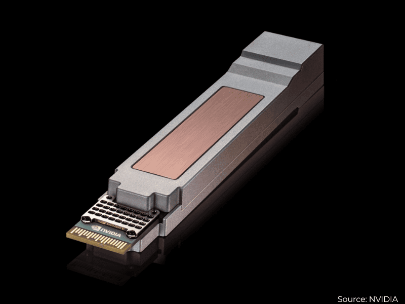
Electronicseng Semiconductors reads the USFP, Ultra-Dense Small Form Factor Pluggable, effort from NVIDIA and Cisco as a connector, optics, and supply-chain move aimed at 400 Gb/s-per-lane AI factories. The partners describe a form factor intended to support links up to 12.8 Tb/s, increase bandwidth density by four times versus present 200 Gb/s-per-lane pluggable optics, and improve power efficiency by approximately 1.3 times. For European data center operators, network equipment makers, and optical component suppliers, the design turns AI infrastructure growth into a test of front-panel density, thermal behavior, and ecosystem interoperability.
Stated technical targets and data citations
The value proposition is not framed as a single speed jump. The companies report that USFP provides four times the bandwidth and front-panel bandwidth density of existing 200 Gb/s-per-lane pluggable modules, plus approximately 1.3 times better power efficiency, while reaching capacity of up to 12.8 Tb/s. Those figures give engineers and procurement teams a concrete way to compare AI fabric expansion against existing pluggable optics assumptions.
- Initial transceivers are planned to pack 16 full-duplex lanes into an OSFP-sized footprint, serving both switches and SuperNICs.
- Later variants may grow to 32 lanes or more.
- USFP modules can dissipate up to 100W without a dedicated embedded cooling circuit.
- Electrical signaling at 400 Gb/s per lane is supported, and performance at 200 Gb/s is also improved.
Data cited from the partners: the four times bandwidth density claim, the approximately 1.3 times efficiency claim, the 16 full-duplex lanes packaging claim, the 32 lanes future claim, the 100W dissipation claim, and the 12.8 Tb/s capacity claim are all presented as part of the USFP design case.
Why connector geometry is the semiconductor-level story
The central innovation is a two-dimensional array connector with a two-step insertion mechanism. High-speed electrical contacts engage only after the module is inserted, which helps reduce contact wear, improve signal integrity, and provide more predictable insertion force. This is where mechanical packaging, semiconductor signal integrity, and field serviceability meet: a denser front panel is only useful if the connection process remains repeatable at speed.
The architecture also supports optical technologies that simplify signal processing to reduce latency and power consumption, while accommodating different connection distances. For switch designers, the stated 100W thermal ceiling without a dedicated embedded cooling circuit may simplify enclosure and board planning. For module vendors, the same requirement places tighter constraints on housing, thermal interface, and contact reliability.
Executive quote that frames the goal
“Building the world’s largest AI factories starts with rethinking the smallest of connections,” said Gilad Shainer, senior vice president NVIDIA. “With USFP, NVIDIA and Cisco are building an ecosystem to reinvent pluggable optics — connecting more computing with greater efficiency to power the next generation of AI factories.”
Comparison table: reference optics versus USFP statements
| Attribute | Reference in the 200 Gb/s-per-lane context | USFP statement |
|---|---|---|
| Bandwidth and front-panel density | existing 200 Gb/s-per-lane pluggable modules | four times |
| Power efficiency | existing 200 Gb/s-per-lane pluggable modules | approximately 1.3 times better |
| Initial packaging | OSFP-sized footprint for switches and SuperNICs | 16 full-duplex lanes |
| Future lane count | later variants may grow | 32 lanes or more |
| Thermal dissipation | module thermal envelope | up to 100W without a dedicated embedded cooling circuit |
Ecosystem, open specification, and supply-chain impact
With TE Connectivity and Amphenol, NVIDIA and Cisco are developing USFP connectors, cages, and modules, and more partners are expected to join. The firms also intend to create an open industry specification through a community-led multi-source project, giving component suppliers a common platform for interoperable high-density optical hardware. The effort extends existing collaboration between NVIDIA Spectrum-X Ethernet networking and Cisco Silicon One-based networks, targeting AI infrastructure deployments across enterprises, neocloud providers, and sovereign cloud operators.
This ecosystem layer matters for semiconductor and hardware procurement because a new form factor only creates value when cages, connectors, modules, and qualification paths are available from multiple sources. It may also create openings for connectivity manufacturers as Ethernet networks shift toward higher density. For European AI infrastructure developers, the proposed standard may offer a more flexible route to higher-bandwidth networking while preserving the serviceability and deployment advantages of pluggable optics.
Selection checklist for AI optics planning
- Confirm whether the planned network uses 400 Gb/s-per-lane objectives or remains centered on 200 Gb/s-per-lane optics.
- Compare the current front-panel density with the four times bandwidth density target and the up to 12.8 Tb/s capacity statement.
- Verify whether switches and SuperNICs can fit the planned 16 full-duplex lanes into an OSFP-sized footprint.
- Review future capacity using the 32 lanes or more variant outlook.
- Check thermal designs against the 100W dissipation target without a dedicated embedded cooling circuit.
- Inspect connector reliability assumptions using the two-dimensional array connector and two-step insertion mechanism.
- Ask suppliers about support for TE Connectivity and Amphenol components, community-led multi-source specification, and interoperable high-density optical hardware.
- Track European supply-chain readiness for data center operators, network equipment makers, and optical component suppliers.
FAQ
What is USFP?
USFP stands for Ultra-Dense Small Form Factor Pluggable. It is an optical transceiver form factor aimed at 400 Gb/s-per-lane connectivity in next-generation AI factories.
How dense is the initial module plan?
The initial transceiver plan is to pack 16 full-duplex lanes into an OSFP-sized footprint, serving both switches and SuperNICs. Later variants may grow to 32 lanes or more.
Why does the connector matter more than speed alone?
Because the stated design relies on a two-dimensional array connector and a two-step insertion mechanism. High-speed contacts engage after insertion to reduce wear, improve signal integrity, and provide more predictable insertion force.
What is the power and thermal claim?
The partners report approximately 1.3 times better power efficiency versus existing 200 Gb/s-per-lane pluggable modules, and they state that USFP modules can dissipate up to 100W without a dedicated embedded cooling circuit.
Who is building the ecosystem?
NVIDIA and Cisco are working with TE Connectivity and Amphenol on connectors, cages, and modules, while expecting more partners to join a community-led multi-source specification.
Common misconceptions
- A common misconception is that 400 Gb/s per lane is only about faster optics. The USFP case also centers on connector geometry, thermal behavior, and multi-source ecosystem availability.
- Another misconception is that higher density necessarily requires a separate embedded cooling circuit for every module. The stated design supports up to 100W without a dedicated embedded cooling circuit.
- A third misconception is that only two large system vendors can define the path. TE Connectivity and Amphenol are named as collaborators, and the partners intend an open industry specification.
- Finally, higher bandwidth does not erase the importance of serviceability. The source frames USFP as a way to reach higher density while preserving the serviceability and deployment advantages of pluggable optics.
Action recommendations
- Start AI fabric optics reviews by mapping 400 Gb/s-per-lane link targets against existing 200 Gb/s-per-lane front-panel assumptions, then compare the four times density claim and the up to 12.8 Tb/s capacity statement.
- Evaluate system packaging around 16 full-duplex lanes in an OSFP-sized footprint for switches and SuperNICs, and test whether future 32 lanes variants would change board layouts or enclosure budgets.
- Treat the two-dimensional array connector and two-step insertion mechanism as a qualification item, not a background detail, because contact wear, signal integrity, and predictable insertion force affect field reliability.
- Require suppliers to describe how they support the ecosystem goals: TE Connectivity and Amphenol involvement, community-led multi-source specification, and interoperable high-density optical hardware.
- For European operators and equipment makers, use the open optics direction as a procurement checkpoint: it may create openings as Ethernet networks move toward higher density, while the existing NVIDIA Spectrum-X Ethernet and Cisco Silicon One collaboration points to broader AI infrastructure alignment across enterprises, neocloud providers, and sovereign cloud operators.