
Inside the RX74M and RX74N: How a 22-nm MRAM Semiconductor Step Reshapes Industrial MCU Design
By Rachel Williams — Electronics & Engineering / Electronicseng Semiconductors desk
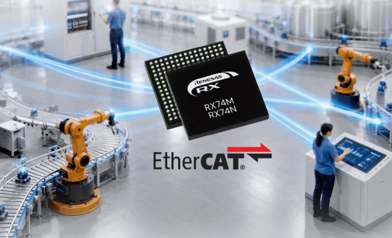
Control-loop designers spend most of their optimization budget on two stubborn bottlenecks at once: the compute ceiling of the core and the erase-before-write penalty of on-chip non-volatile code storage. Renesas is now addressing both inside a single silicon step. The RX74M and RX74N arrive as the first 32-bit MCUs in the RX family to combine a 22-nm semiconductor process with embedded MRAM, each built around a 600-MHz RXv3e core. From a Semiconductors desk standpoint the launch is less a catalog addition than a preview of where industrial control silicon is heading: deterministic memory paths, networking hardware moved on-chip, and firmware update behavior that no longer inherits flash-era constraints.
1. What the 22-nm node and the RXv3e core change at board level
Shifting the RX line to a 22-nm process is the enabling decision behind the embedded MRAM integration and the 600-MHz clock target. For a hardware team the practical consequence is that performance headroom and a reworked memory architecture land together instead of being traded against each other. The CPU is the RXv3e, and both parts are positioned as industrial devices rather than general-purpose controllers.
The reference point given in the announcement is explicit: against the 240-MHz RX72M and RX72N, the new pair delivers more than twice the performance. A raw clock ratio does not tell the whole story — core generation, wait-state behavior and the tightly coupled memory path all shape achieved throughput — but for planning purposes the conclusion is simple. Loops that previously consumed most of a 240-MHz budget now have headroom, and functions that were split across an MCU plus a companion device become candidates for consolidation on one chip.
2. Memory architecture: MRAM, TCM RAM and SRAM each do a different job
Every device provides 1 MB of code MRAM, 256 KB of zero-wait-state tightly coupled memory (TCM) RAM, and 1.5 MB of SRAM aimed at real-time processing. Collapsing these three blocks into a single "memory budget" number is where selection mistakes begin.
| Memory block | Capacity on each part | Role in a control design |
|---|---|---|
| Embedded MRAM (code) | 1 MB | Program storage that can be written without a prior erase cycle, so code and data updates can be faster and programming time is reduced |
| TCM RAM | 256 KB, zero wait state | Time-critical routines and data placed on a deterministic path next to the core, avoiding shared-bus arbitration jitter |
| SRAM | 1.5 MB | Working memory for stacks, communication queues, buffers and real-time data structures |
Why "no erase" is more than a convenience feature
With embedded flash, writing cells normally requires erasing the surrounding block first, which forces designers into staging areas, wear-aware update algorithms and long programming windows. Because MRAM can be written without a prior erase operation, unlike embedded flash, both the in-field update procedure and the production programming step get shorter, and the same non-volatile array can hold code alongside frequently updated data without the erase-block gymnastics flash imposes.
One caution for reliability and sourcing reviewers: endurance, retention and security characteristics beyond the erase-free write behavior are not part of this announcement, so confirm those figures in the device documentation before committing a field-updatable product to the architecture.
3. Performance and process data to carry into a selection review
- Core: RXv3e running at 600-MHz on both parts.
- Relative gain: more than twice the performance of the 240-MHz RX72M and RX72N.
- Memory stack: 1 MB code MRAM + 256 KB zero-wait-state TCM RAM + 1.5 MB SRAM.
- Process: 22-nm — a first for the RX family together with embedded MRAM.
- Baseline connectivity on both: Gigabit Ethernet and CAN FD.
- Positioning: 32-bit industrial MCUs, not consumer-grade parts.
The connectivity bullet is easy to under-read. On-chip Gigabit Ethernet plus CAN FD sharing a 600-MHz core means protocol stacks compete with the control loop for the same silicon, which is precisely where the zero-wait-state TCM block and the 1.5 MB SRAM pool justify their presence.
4. RX74M versus RX74N: choosing the right half of the pair
Core, memory and the base networking set are common to both. The RX74M layers additional industrial networking hardware on top: a TSN-capable Ethernet switch and an EtherCAT slave controller.
| Parameter | RX74M | RX74N |
|---|---|---|
| CPU / clock | RXv3e at 600-MHz | RXv3e at 600-MHz |
| Code MRAM | 1 MB | 1 MB |
| TCM RAM | 256 KB, zero-wait-state | 256 KB, zero-wait-state |
| SRAM | 1.5 MB | 1.5 MB |
| Gigabit Ethernet | Integrated | Integrated |
| CAN FD | Integrated | Integrated |
| TSN-capable Ethernet switch | Added | Not listed for this part |
| EtherCAT slave controller | Added | Not listed for this part |
| Target equipment | AC drives, industrial robots, PLCs | Smart meters, power conditioners, HVAC systems |
Application reading
For servo-class work — AC drives, industrial robots and PLCs — the RX74M is the designated part, and the TSN-capable switch plus EtherCAT slave controller line up with the deterministic, multi-node expectations of automation networks. For metering and power-distribution equipment — smart meters, power conditioners and HVAC — the RX74N keeps the same 600-MHz core and memory stack while dropping the automation fieldbus extras, which holds the bill of materials closer to the traffic profile those products actually generate.
5. Where these parts sit in the semiconductor value chain
Embedded MRAM on a 22-nm logic process is an integration decision made at the wafer level, and it pulls two functions that many boards previously separated — program storage and fast update capability — into the MCU itself. For procurement and system architects, the interesting second-order effect is part-count compression: with 1 MB of code MRAM, 256 KB of zero-wait-state TCM RAM, 1.5 MB of SRAM, Gigabit Ethernet, CAN FD and, on the RX74M, a TSN-capable switch and EtherCAT slave controller all on-chip, discrete network processors and external serial memory become candidates for removal rather than default BOM items. That changes qualification scope, test coverage at assembly, and the failure analysis path, so it should be reviewed as a system-level change and not just a microcontroller swap.
6. Selection checklist for the first design-in cycle
- Measure the current loop execution time on a 240-MHz class part such as the RX72M or RX72N, then repeat the same benchmark on the new core so the "more than twice" figure is validated against your workload instead of a marketing sheet.
- Split the memory plan across three domains: program image in 1 MB code MRAM, critical routines and data in 256 KB zero-wait-state TCM RAM, buffers and stacks in 1.5 MB SRAM.
- Fix the network contract early: equipment that must join a TSN domain or behave as an EtherCAT slave points to the RX74M; traffic limited to Gigabit Ethernet and CAN FD is covered by both, including the RX74N.
- Redraw the firmware update flow to exploit erase-free writes rather than porting a flash-era staging scheme unchanged.
- Request the evaluation hardware — the parts are available now, and corresponding evaluation boards are also available.
- Close the documentation loop with Renesas Electronics datasheets for the parameters this announcement does not cover before locking a field-updatable design.
7. Common misconceptions to avoid
- "MRAM is simply faster flash." The defining property here is write-without-erase; assuming the array is a drop-in replacement with identical tooling and update assumptions wastes the redesign opportunity.
- "600-MHz automatically closes the loop budget." Achieved loop time still depends on how much code and how many critical data structures live in the zero-wait-state path versus shared memory.
- "The two variants are interchangeable." The RX74M adds the TSN-capable Ethernet switch and the EtherCAT slave controller that the RX74N is not described as carrying.
- "A first for MRAM means the idea is untested." The claim is scoped: these are the first 32-bit MCUs in the RX family to use a 22-nm process together with embedded MRAM.
- "More on-chip memory means more headroom for everything." The performance boundary that matters is real-time determinism; capacity without deterministic access would not help a servo or metering task.
8. Action recommendations
- Run a migration assessment on one live program that currently sits on 240-MHz hardware, using the RX74M or RX74N evaluation board as the comparison vehicle.
- Assign TCM ownership explicitly in the software architecture review, so the 256 KB zero-wait-state block is reserved for loop-critical code instead of being treated as overflow SRAM.
- If your equipment roadmap includes automation networks, standardize on the RX74M to keep the TSN and EtherCAT options open without a second silicon change later.
- Treat the erase-free write behavior as a product feature: revisit service-tooling time, update reliability and in-field data logging flows.
- For energy-metering and HVAC platforms, keep the RX74N as the default and challenge any request to add automation fieldbus hardware that the application does not use.
FAQ
Are the RX74M and RX74N available for design-in?
Yes. Both are listed as available now, and corresponding evaluation boards are also available, which makes benchmarking on real workloads feasible within the current design cycle.
What makes these the technical first for the RX family?
They are the first 32-bit MCUs in the RX family to use a 22-nm process and embedded MRAM, with the RXv3e core running at 600-MHz.
How much on-chip memory is provided?
Each part carries 1 MB of code MRAM, 256 KB of zero-wait-state TCM RAM and 1.5 MB of SRAM.
Is the update advantage really about erase cycles?
That is the stated mechanism. MRAM can be written without a prior erase operation, unlike embedded flash, so code and data updates can be faster and programming time is reduced.
Which part supports EtherCAT and TSN?
The RX74M adds the TSN-capable Ethernet switch and the EtherCAT slave controller. Both devices integrate Gigabit Ethernet and CAN FD.
What performance gain should a migrating team expect?
The published comparison is more than twice the performance of the 240-MHz RX72M and RX72N. Treat that as a planning figure and confirm with your own code, because wait states, stack placement and networking load all affect achieved loop time.
Which applications are targeted?
The RX74M is intended for industrial automation equipment such as AC drives, industrial robots and PLCs; the RX74N targets smart meters, power conditioners and HVAC systems.
Bottom line
For engineers tracking semiconductor roadmaps in factory automation and energy infrastructure, the pair signals three shifts worth planning around: process-node progress that finally brings embedded MRAM to a mainstream 32-bit control core, a memory structure tuned for real-time determinism instead of headline capacity, and networking silicon absorbed into the MCU where the application justifies it. Choose the RX74M when deterministic fieldbus participation is part of the product story; choose the RX74N when the same 600-MHz core and 1 MB code MRAM, 256 KB zero-wait-state TCM RAM and 1.5 MB SRAM are what the equipment actually needs, without the extra automation interfaces.