
Silicon Program Math: What the Siemens and NVIDIA GPU Patterning Numbers Change for High-NA EUV Teams
Ask a design-for-manufacturing lead where an advanced-node program really loses weeks, and the answer is rarely a queue at the mask shop or a booking sheet on the tool floor. It is the simulation calendar: how many full-chip patterning passes a team can afford before tapeout locks. Read that way, the expanded collaboration between Siemens and NVIDIA stops being a vendor headline and becomes a planning input. The published range, at least 10x to 17x faster simulation on key lithography workloads, rewrites the arithmetic behind optimization depth, hotspot discovery timing and process margin recovery.
Technically the pairing is narrow and deliberate. NVIDIA cuLitho, a CUDA-X library written for GPU-accelerated computational lithography, is combined with Calibre, the Siemens manufacturing software already used for patterning sign-off. The target is the segment of the flow that has been resisting schedule pressure for years, the constraint the partners call the runtime wall. What follows is the Electronicseng Semiconductors desk read of how that change lands for DFM teams, mask operations and the buyers who depend on both.
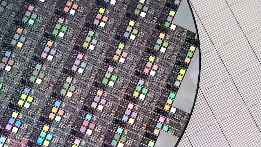
The bottleneck, stated in engineering terms
Patterning complexity climbs with every push toward leading-edge process nodes, and the climb is not linear. Two demands do most of the damage. High-NA EUV shifts the optical regime and pushes simulation fidelity upward, so models that were adequate one generation back now have to resolve more, across more of the layout. Curvilinear methods such as Inverse Lithography Technology (ILT) compound the problem: they are inherently iterative, treating each mask shape correction as a computation-heavy optimization rather than a lookup. Conventional optical proximity correction (OPC) and classical computational lithography workflows were scoped for a world in which neither condition held at full-chip scale.
What falls out is a scheduling problem disguised as a compute problem. Without acceleration, these essential techniques are frequently too slow for full-chip, manufacturing-scale deployment, so engineering teams are pushed into a forced trade between optimization depth and project schedule. That trade is not neutral. Unexamined regions of the layout stay unresolved, lithographic hotspots surface late, process margins shrink, and the yield penalty concentrates in precisely the devices with the least tolerance for it, namely the most advanced AI compute and memory parts.
Reading the stack layer by layer
The scope of the integration is deliberately tight, which is why it is readable as engineering news rather than marketing noise.
- NVIDIA cuLitho: the CUDA-X library component. Its role in the announcement is to carry computational lithography workloads onto GPU parallelism instead of leaving them in CPU-bound batch simulation.
- Siemens Calibre: the manufacturing software layer where OPC and computational lithography verification already live, and where the output feeds tapeout decisions.
- The integration point: pairing the two attacks runtime, not the invention of a new correction model. The value proposition is running more of a workflow you already trust, over more of the chip, inside the window you already have.
The data, and the scope attached to it
Verified engineering data reported by the partners supports simulation speed-ups ranging from at least 10x to 17x for key lithography simulation workloads. The floor of the claim is at least 10x acceleration on those workloads; the published ceiling for the measured cases is 17x.
Scope matters more than the headline multiple. The figures are attached to named simulation workloads inside computational lithography, not to every job in a design-to-manufacturing flow, and not to unrelated EDA tasks. The useful interpretation is a schedule lever on the patterning verification segment, with all downstream effects derived from having more simulation cycles available.
| Program dimension | Behaviour under runtime-limited simulation | What the reported 10x to 17x range changes |
|---|---|---|
| Iteration budget | Optimization depth traded against the calendar | More passes completed in less time |
| Hotspot discovery | Surfaces late, close to sign-off | Potential hotspots identified before tapeout |
| Full-chip curvilinear work (ILT-class) | Too slow for manufacturing-scale deployment | Practical for High-NA EUV production |
| Process margin | Thin headroom, yield risk concentrated in advanced AI compute and memory devices | Margin improved ahead of tapeout |
| Program stage | Manufacturing readiness lags silicon availability | Faster turnaround, supporting deployment of new AI silicon |
| Who benefits | Verification capacity caps both sides of the chain | Measurable gains named for semiconductor and mask manufacturers |
One caution for anyone building a business case on this. The reported multiples describe simulation runtime on the named workload classes. They do not describe a guaranteed yield uplift, a fixed tapeout date, or a specific hardware configuration. Treat 10x to 17x as evidence that a constraint has moved, then measure the effect inside your own flow before restating it as a program commitment.
Where acceleration converts into schedule value
- Iteration count. Shorter runs mean more correction passes inside the same calendar window, which turns ILT-style optimization from a sampling exercise into something closer to full coverage.
- Hotspot timing. The stated benefit is identifying potential hotspots before tapeout, which moves the cheapest fix window earlier in the program.
- Margin recovery. Fuller and earlier optimization leaves more distance between the printed result and the specification, instead of leaving margin to be recovered through late rework.
- Mask-side planning. Because mask manufacturers are named as beneficiaries, review cadence and data expectations can be planned around accelerated verification rather than a sparse sample set.
- Readiness for AI silicon. Faster turnaround on the verification segment supports the deployment of next-generation AI semiconductors as manufacturable products, which is the market this collaboration points at.
Common misreadings to avoid
Myth one: every job in the flow now finishes 17x faster
The published numbers are attached to key lithography simulation workloads. Other stages of a design-to-manufacturing flow sit outside the stated scope, and no figure in the reported range should be copied onto them.
Myth two: this is an EDA tool story with no fab consequence
The value statement runs all the way to manufacturability: moving past runtime-limited constraints in advanced patterning so that next-generation AI semiconductors can become manufacturable products.
Myth three: curvilinear methods are optional polish
ILT is described as one of the techniques the industry needs, not one it would like to have. Without acceleration such methods are frequently too slow for manufacturing-scale deployment, so compute capability, not preference, decides whether they are used at full-chip scale.
Myth four: only device makers are in scope
Mask manufacturers are explicitly named alongside semiconductor makers as recipients of measurable gains across critical computational lithography workflows. Supply-chain readers should treat mask operations as a first audience.
Myth five: memory products sit outside the risk
Yield exposure is called out for the most advanced AI compute and memory devices alike. Teams on memory roadmaps have the same hotspot and margin problem, and the same benefit from a longer effective iteration budget.
Action checklist by role
DFM and computational lithography leads
- Establish a local baseline: record current full-chip simulation runtimes for the OPC and ILT-class passes you actually run, so the 10x to 17x claim can be compared with your own data rather than a press range.
- Re-budget iterations before hours: convert saved runtime into extra correction passes and hotspot review cycles first, and into calendar compression only second.
- Pull the hotspot sign-off gate earlier in the plan and define a re-entry path for layouts that fail it.
- Track margin, not just speed: log process-window headroom per iteration so the acceleration is proven by outcome, not only by clock time.
Mask operations
- Re-plan review cadence around denser simulation output instead of the sparse pass set that runtime limits previously allowed.
- Confirm which verification artifacts are shared between device maker and mask shop, and which are regenerated locally.
- Include simulation turnaround as an explicit variable in mask data scheduling for High-NA EUV programs.
Procurement and supply chain
- Treat verification throughput as a capacity factor when scheduling advanced AI compute and memory parts, not only wafer starts.
- Ask suppliers which portion of their computational lithography flow is accelerated, and where the at least 10x floor is claimed.
- Do not price yield promises into contracts on the strength of a simulation multiple alone.
FAQ
Are these projections or measured results?
Measured. The partners cite verified engineering data supporting simulation speed-ups in the range of at least 10x to 17x for key workloads, with the low end stated as at least 10x acceleration.
What exactly is being combined?
NVIDIA cuLitho, a CUDA-X library built for GPU-accelerated computational lithography, paired with Calibre, the Siemens manufacturing software. The combination targets the runtime wall that gates advanced chip patterning.
Which patterning problems drive the compute demand?
Two, according to the description: the move to High-NA EUV, and the need for advanced curvilinear methods such as Inverse Lithography Technology.
Does a mask house benefit even if it does not design chips?
Yes. Mask manufacturers are named as a beneficiary group, with gains measured across critical computational lithography workflows rather than only across device design.
Does this shorten tapeout?
Not automatically. The mechanism is more iterations in less time and earlier hotspot detection, which typically reduces late-stage rework; faster turnaround can therefore help accelerate manufacturing readiness, but the calendar effect still has to be validated in a specific flow.
Why is AI silicon the reference market?
Because runtime-limited constraints in advanced patterning are what stand between next-generation AI semiconductor designs and manufacturable products, and because yield risk is concentrated in the most advanced AI compute and memory devices.
The Electronicseng take
For most engineering readers the immediate action is not to repeat the multiple, it is to change what the schedule assumes. Patterning verification has long been the segment where ambition met the calendar, and where depth quietly surrendered to deadlines. If the reported numbers hold inside your own flow, the scarce resource stops being simulation time and becomes engineering attention: more passes to review, more hotspot candidates to disposition, more margin decisions to make before sign-off. That is a staffing and process problem rather than a compute problem, and teams that plan for it now will be the ones who actually convert the speed-up into yield.