
Electronicseng Semiconductors: Sony LYTIA 720 Main-Camera Sensor Uses 1/1.56-inch, 50 MP Stacked CMOS to Push 4K HDR Video
The smartphone main camera is becoming a system-level semiconductor decision, not a simple part swap. In the Semiconductors column at Electronicseng, Sony Semiconductor Solutions Company’s announcement of Sony LYTIA 720 is read through that lens: a stacked CMOS image sensor placed in the widely used 1/1.56-inch format, carrying approximately 50 million effective pixels, 1.0 micrometer pixels, and an approx. 10.24 mm diagonal. Its stated mass production and shipment window is early November 2026. That timing gives camera module, ISP, lens, and mobile platform teams a planning signal while preserving enough specification detail for technical comparison with prior parts in the LYTIA series.
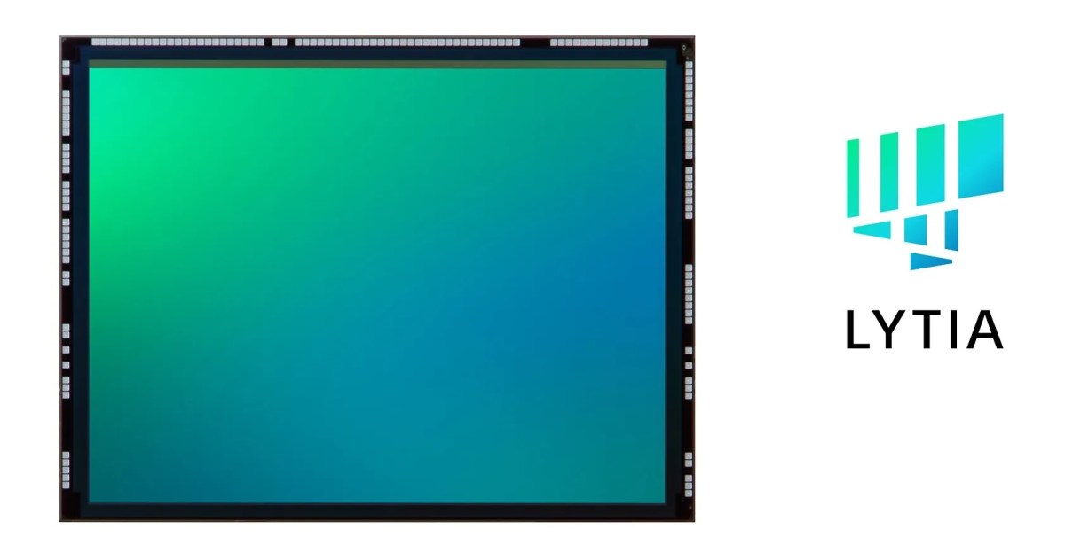
What Sony Is Trying to Solve in the 1/1.56-inch Main-Camera Segment
The LYTIA series sits in Sony’s higher-end image-sensor positioning, and LYTIA 720 continues several core technical themes while aiming its main improvements at low-light imaging, autofocus, and dynamic range. The headline target is the smartphone main camera, a subsystem where mechanical space, power budget, thermal limits, and lens compatibility constrain every added transistor or pixel operation. Because the stated format is 1/1.56-inch, engineers must interpret the device not as a large-sensor replacement strategy, but as an optimization within a very common mobile camera envelope.
According to the published description, Sony LYTIA 720 uses a stacked CMOS architecture and UHCG, Sony’s ultra-high conversion gain circuit. The practical meaning of UHCG is that charge-to-voltage conversion efficiency is improved. In the same optical format, the company states that low-light random noise can be reduced by about 50% versus LYTIA 700. That is a meaningful signal for dark scenes and dim indoor capture because random noise and grain directly affect the detail that later image-processing stages can recover. The reported improvement is not framed as an absolute quality jump in every lighting condition; it is a noise-path improvement within a specified size and pixel pitch.
Reported Specification Data and Source Context
For design and procurement discussions, the useful approach is to separate stated parameters from implied system effects. The following table collects the numerical and identity anchors that appear in the Sony Semiconductor Solutions Company description. It should not be read as a complete datasheet; it is a content-level summary for comparison planning.
| Item | Reported value | Why it matters |
|---|---|---|
| Product | LYTIA 720 | Identifies the next-generation LYTIA series part targeted at main cameras. |
| Announcing company | Sony Semiconductor Solutions Company | Links the sensor to Sony’s mobile CMOS image-sensor portfolio. |
| Effective pixels | Approx. 50 million effective pixels | Supports main-camera resolution while leaving cropping and processing decisions to the platform. |
| Optical format | 1/1.56-inch | Keeps the sensor in a widely adopted phone-main-camera footprint. |
| Diagonal length | Approx. 10.24 mm | Helps camera-module and lens-stack engineers estimate physical integration. |
| Pixel size | 1.0 micrometer | Sets the native sampling pitch and influences low-light charge collection. |
| Noise claim | About 50% lower random noise in low light versus LYTIA 700 | Indicates a cleaner raw signal for dark scenes and supports later detail recovery. |
| Video capability | 4K 60-frame HDR video | Places LYTIA 720 in the segment where autofocus and HDR video must operate together. |
| Video capability notation | 4K 60fps HDR video | Matches the fps-based way many platform and module teams discuss mobile video. |
| Dynamic range | Up to 100dB dynamic range with Hybrid Frame-HDR | Targets highlight and shadow preservation while reducing reliance on multi-frame capture. |
| Production plan | Early November 2026 | Gives product planners a concrete manufacturing and shipment milestone. |
AF, ADC Redesign, and the 4K HDR Video Claim
For video pipelines, LYTIA 720 is described as the first Sony product in the 1/1.56-inch size and 1.0 micrometer pixel-size class to combine full-pixel autofocus with 4K 60-frame HDR video. That combination is important because the sensor is asked to support both focus responsiveness and HDR video operation in the same readout environment. Sony says it redesigned and optimized the analog-to-digital conversion AD circuit, reducing conversion latency and power. These changes are presented as enabling the simultaneous support of fast autofocus and HDR video capture.
The product also uses a Quad Bayer color filter array, a pattern commonly discussed for smartphone main cameras. The published description emphasizes 4K 60fps HDR video, full-pixel autofocus, high-speed image output, and quality-aware power management. For engineers, this suggests the sensor is positioned for main-camera use cases where still capture, motion video, and autofocus must share the same readout budget. Avoid assuming features not listed; integration depends on ISP firmware, lens optics, thermal design, and platform tuning.
Single-Frame HDR, Hybrid Frame-HDR, and the 100dB Dynamic Range Path
Traditional multi-frame HDR synthesis can produce ghosting and trailing when subjects or the camera move. In a main camera, that problem is especially visible in handheld video or fast panning. LYTIA 720 is described as moving to a single-frame HDR method, which is intended to maintain fast autofocus response while still supporting HDR video capture. The goal is smoother dynamic scenes, because the sensor is not relying on merging several temporally separated frames.
For still imaging and HDR processing, the part supports Hybrid Frame-HDR and states a maximum 100dB dynamic range. The described method combines DCG-HDR data from a single exposure with high-brightness region data captured with a short exposure, then uses post-merging to preserve shadow and highlight information. In practice, that targets common failure modes of mobile main cameras: crushed dark areas and clipped highlights in mixed indoor and outdoor lighting. Final image quality will depend on tone mapping, motion handling, and the surrounding processing chain.
| Comparison axis | Traditional multi-frame HDR | LYTIA 720 described HDR path |
|---|---|---|
| Temporal behavior | Uses several frames; motion between frames can create ghosting and trailing. | Uses a single-frame HDR approach aimed at faster autofocus response and more natural motion. |
| Video relevance | May be harder to reconcile with high-speed capture and moving scenes. | Described as supporting 4K 60fps HDR video while avoiding multi-frame artifacts. |
| Dynamic-range strategy | Relies on exposure bracketing and merging. | Hybrid Frame-HDR combines DCG-HDR data with short-exposure bright-area data, up to 100dB dynamic range. |
| Design trade-off | Can be strong for static scenes, but sensitive to motion. | Seeks to preserve shadow and highlight detail while making video less dependent on frame merging. |
Selection Checklist for Engineers and Procurement Teams
- Confirm whether the target main camera actually uses a 1/1.56-inch module envelope, with lens and actuator space compatible with approx. 10.24 mm diagonal placement.
- Map approximately 50 million effective pixels to your JPEG, RAW, and video processing pipeline, especially if the product plan includes cropping, zoom, or high-speed readout.
- Use the 1.0 micrometer native pitch and Quad Bayer pattern as starting assumptions for sensor-mode selection; verify against the full datasheet before committing to output resolution.
- For low-light products, compare the stated about 50% low-light random-noise reduction versus LYTIA 700 as a raw-signal improvement, not as a guarantee of final photo quality after ISP processing.
- Validate the 4K 60-frame HDR video requirement in the SoC ISP path, including buffer depth, thermal throttling, autofocus tuning, and HDR tone mapping.
- Check whether the platform can sustain high-speed image output while maintaining quality and power targets, since the announcement describes these as concurrent goals.
- Treat early November 2026 as a mass-production shipment date for planning; if your project schedule needs samples, bring-up, or reliability qualification earlier, verify the actual sample and delivery timeline through official channels.
Common Misconceptions About LYTIA 720 Reports
- “50 million pixels” is not the whole story. The same resolution can produce different system-level results depending on optical format, pixel pitch, conversion gain, readout architecture, and HDR strategy.
- 1/1.56-inch is a compact mobile format, not a large-format camera sensor. Integration value comes from optimizing within a known smartphone footprint, not from implying that every competing design is outdated.
- 1.0 micrometer pixels are a physical attribute, not a direct score. Noise and dynamic range are shaped by UHCG, AD circuit optimization, Hybrid Frame-HDR, and the complete processing chain.
- “Up to 100dB dynamic range” is a maximum stated capability under Hybrid Frame-HDR. Real capture depends on exposure mode, scene motion, and how the short-exposure and DCG-HDR data are combined.
- 4K 60fps HDR video is a sensor-side capability description. Platform performance, thermals, storage bandwidth, and lens stabilization remain outside the announcement and should not be assumed automatically.
Action Recommendations for Semiconductor Planning
- For smartphone OEM and ODM camera-system teams, add LYTIA 720 to the main-camera candidate list only after optical stack and module geometry validation around 1/1.56-inch and approx. 10.24 mm diagonal.
- For image-quality groups, build A/B tests against LYTIA 700 using low-light random-noise targets and motion-rich HDR scenes, because the two most specific improvements are noise reduction and single-frame HDR behavior.
- For supply-chain planners, align demand forecasts to early November 2026 production shipment, while securing alternate sources and qualification buffers for any schedule risk.
- For product marketing, communicate the capability as system-level: approximately 50 million effective pixels, 1/1.56-inch format, 1.0 micrometer pixels, 4K 60-frame HDR video, full-pixel autofocus, and Hybrid Frame-HDR with up to 100dB dynamic range.
- For technical writers and analysts, avoid speculative claims about device examples, market share, or final phone quality; the current announcement supports only the sensor architecture and performance directions listed above.
FAQ: The Most Frequent Technical Questions
Who announced LYTIA 720?
Sony Semiconductor Solutions Company announced LYTIA 720 as a next-generation image sensor for smartphone main cameras, positioned within the LYTIA series.
What are the core size and pixel numbers?
The sensor uses a 1/1.56-inch format, approximately 50 million effective pixels, a 1.0 micrometer pixel size, and an approx. 10.24 mm diagonal.
How does it improve low-light performance?
Sony states that UHCG improves charge-to-voltage conversion efficiency, and low-light random noise can be reduced by about 50% versus LYTIA 700. That reduces grain and supports better detail in dark scenes.
Why does the 4K HDR video claim matter?
LYTIA 720 is described as the first Sony part in its 1/1.56-inch, 1.0 micrometer pixel-size class to support both full-pixel autofocus and 4K 60-frame HDR video. This matters for main cameras that need fast focus and HDR motion capture together.
What is the production date?
The published plan is early November 2026 for mass production and shipment.
Should designers treat the 100dB dynamic range as a system guarantee?
No. The statement is a sensor-level capability enabled by Hybrid Frame-HDR, with up to 100dB dynamic range. End-to-end image quality still depends on ISP implementation, motion handling, tone mapping, and final module tuning.
Final Engineering Takeaway
The practical value of LYTIA 720 is that it packages several pressure points of the smartphone main camera into one reported platform: 1/1.56-inch integration, approximately 50 million effective pixels, 1.0 micrometer pixels, lower random noise versus LYTIA 700, full-pixel autofocus, 4K 60fps HDR video, and Hybrid Frame-HDR up to 100dB dynamic range, with production planned for early November 2026. For Electronicseng readers working across semiconductor design, imaging systems, and supply planning, the right next step is not to declare a device-level win, but to test how these stated parameters behave inside a complete camera module and mobile platform.