
Electronicseng Semiconductors: Diamond Transistor Work From Stanford University Targets 50x Switching and 3 nm Subthreshold-Swing Parity
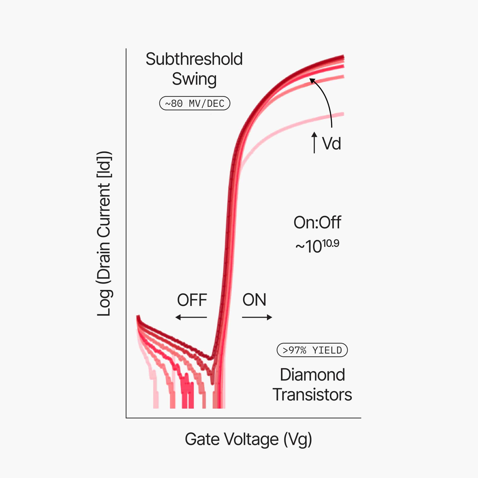
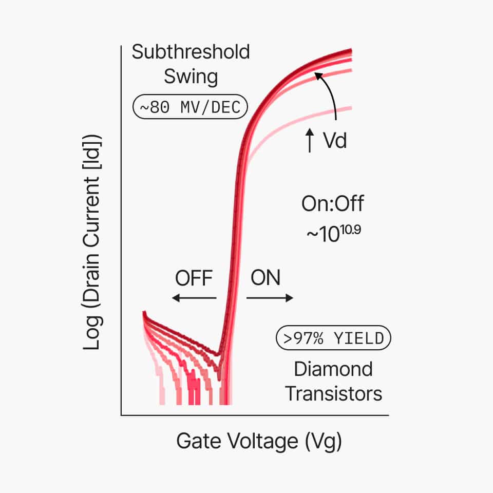
For semiconductor readers, the meaningful update from Electronicseng Semiconductors is a development story centered on Stanford University and diamond transistors, with a 50x switching target. The cited comparator is not a complete device benchmark; it is a subthreshold-swing statement, where DF devices now match state-of-the-art 3 nm silicon.
Signal Map for Semiconductor Engineers
- Development focus: the reviewed material describes all-diamond MOSFETs developed in partnership with Stanford University and frames the work around a 50x faster switching objective.
- Carrier method: DF devices create carriers through surface transfer doping, so substitutional dopant atoms are not placed in the diamond crystal bulk.
- Source anchor: the relevant paper is cited as a DF paper published in IEEE and concerns conduction in diamond 2-Dimensional hole gas field effect transistors.
- Electrostatic comparator: for subthreshold swing, the source reports that DF devices now match state-of-the-art 3 nm silicon.
- Application framing: the mechanism is positioned as attractive for high-power, high-frequency, and radiation-hard electronic device platforms.
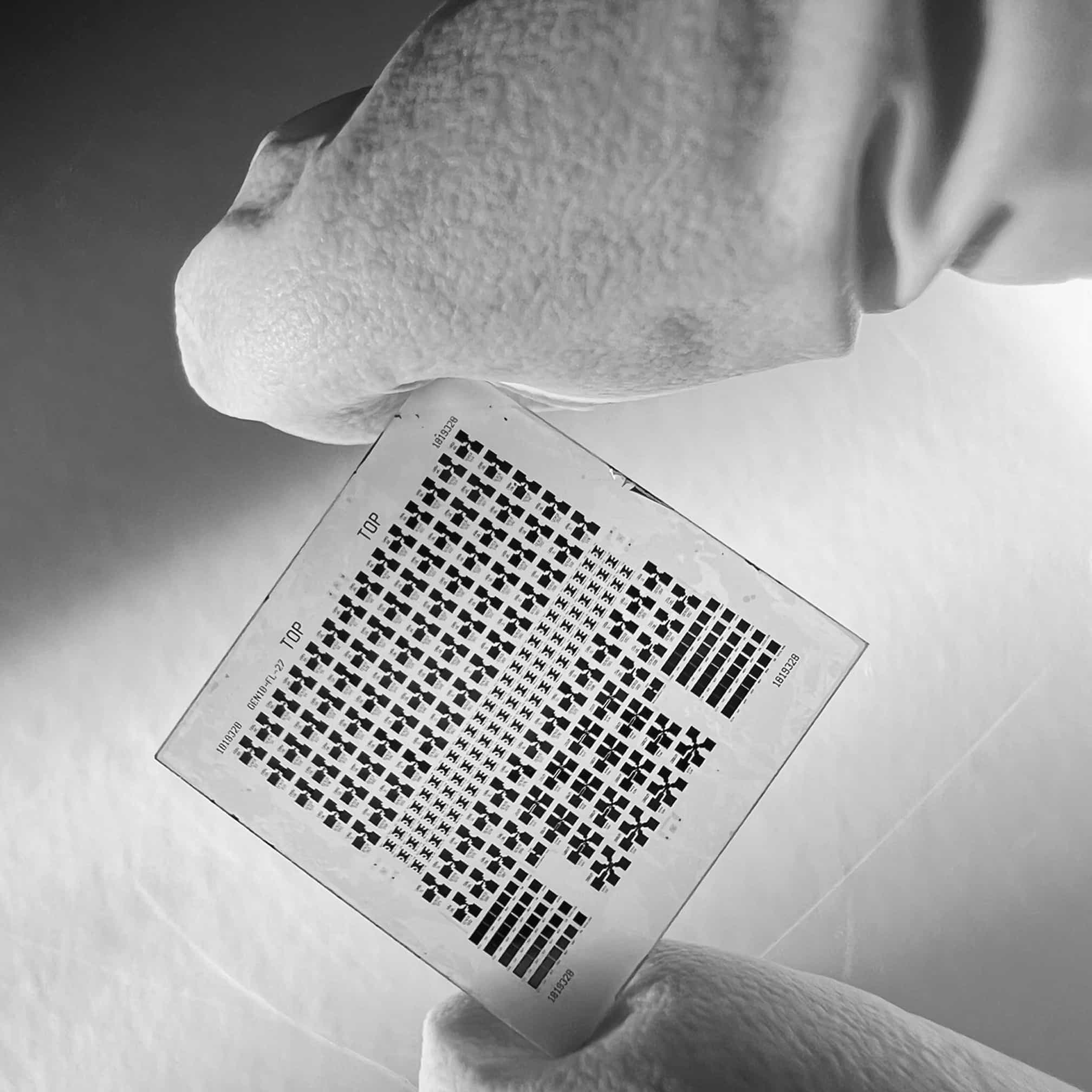
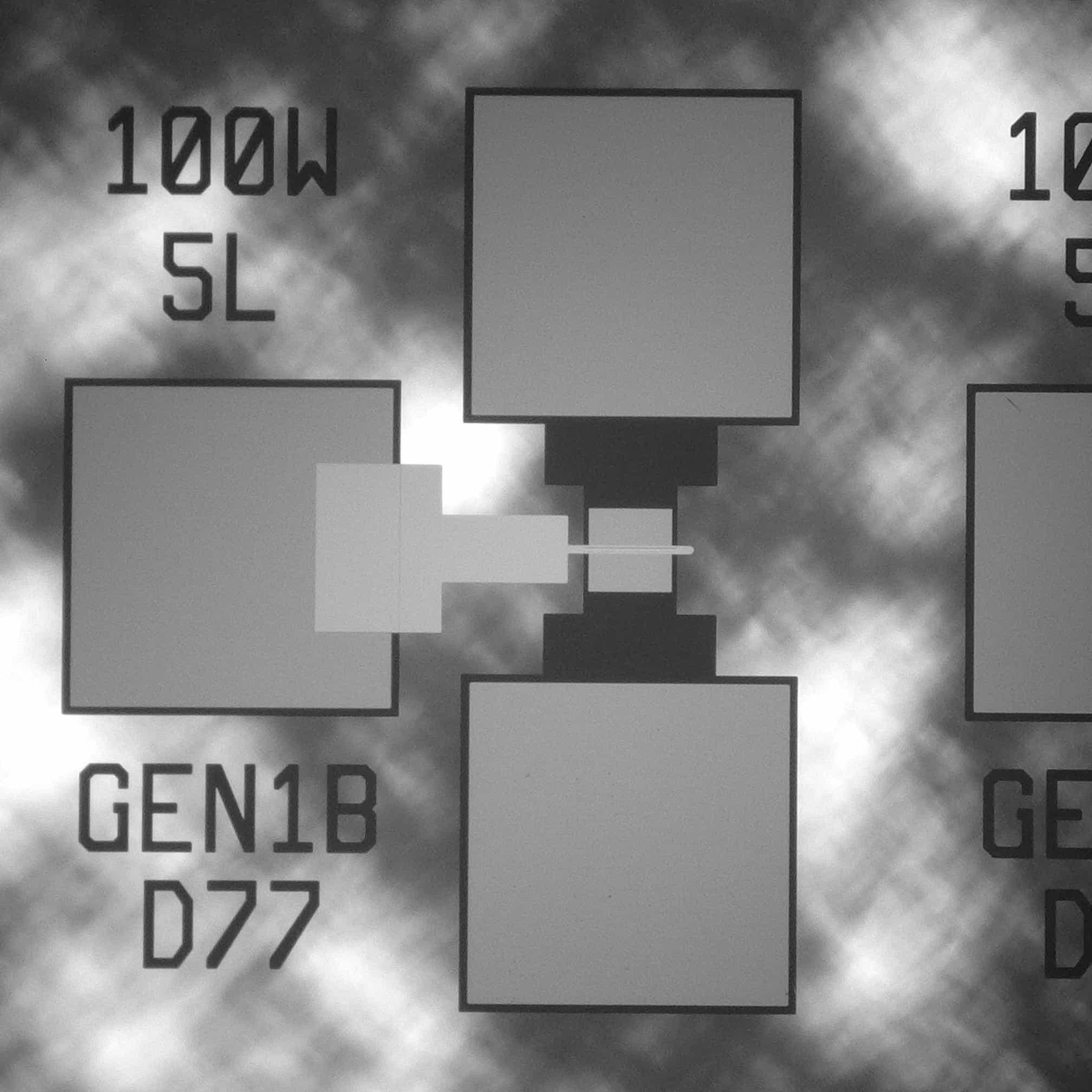
Surface Transfer Doping as the Differentiator
The reported method can be read as a sequence of surface conditions rather than as a conventional dopant recipe. First, the source describes a single-crystal diamond wafer whose surface is terminated with an atomic layer of hydrogen. Second, that hydrogen termination is said to make the surface electron affinity negative. Third, electrons can transfer from the diamond valence band to suitable acceptor species at the surface, including adsorbates or engineered surface layers. Fourth, the transferred charge creates a high-density two-dimensional hole gas, or 2DHG, confined within a few nanometers of the surface.
That fourth step is the key reason the mechanism matters. The device obtains p-type conductivity through a surface-confined hole gas rather than through substitutional doping atoms distributed in the crystal bulk. Because the bulk is not forced to accept dopant atoms in the same way, the reported approach preserves the intrinsic purity, thermal conductivity, and breakdown strength of diamond. For readers evaluating next-generation semiconductor platforms, this changes the engineering tradeoff: surface physics becomes part of device electrostatics, not merely an interface detail.
The source also frames the method as avoiding defects and scattering. It states that neither ion implantation nor lattice substitution is required for the reported surface transfer doping approach, and that this avoids defect generation and carrier scattering associated with conventional doping. That is why the work is linked to high-power, high-frequency, and radiation-hard electronic device platforms. The material does not supply a full device benchmark table, but the mechanism itself is the differentiator to track.
Reading the DF Paper in IEEE
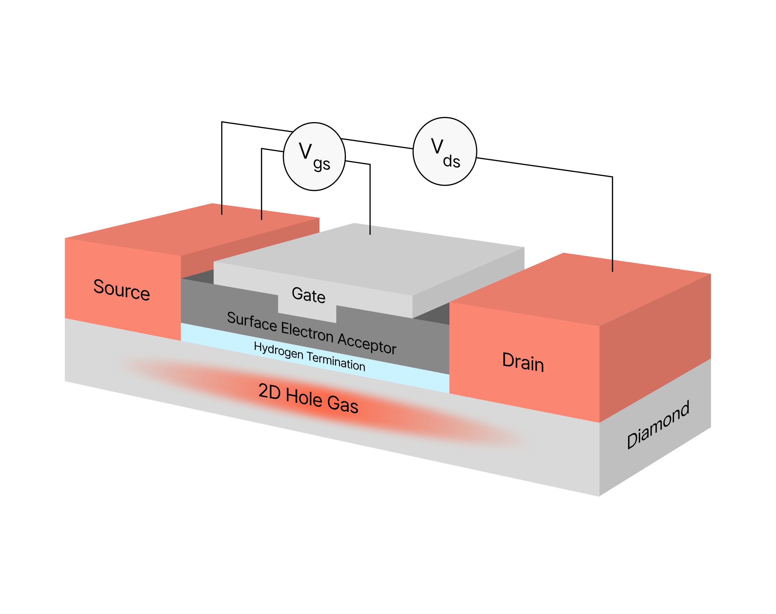
The cited DF Paper in IEEE is the anchor for the conduction mechanism. It links hydrogen termination, negative electron affinity, acceptor-mediated charge transfer, and the 2-Dimensional hole gas story. The value for this column is narrow but useful: it explains how charge carriers can be induced in diamond without placing substitutional dopant atoms into the bulk crystal. In the reviewed summary, the DF devices are described as all-diamond MOSFETs developed in partnership with Stanford University, with 50x faster switching as the target. The IEEE paper anchor should therefore be read as the technical explanation behind the surface-transfer-doping mechanism, not as a standalone product announcement.
Comparison Table: Source-Reported DF Device Logic
| Design Question | Source-Reported Answer | Engineering Reading |
|---|---|---|
| Where are carriers created? | At or near a hydrogen-terminated diamond surface, through surface transfer doping. | Surface termination and acceptor species are part of channel formation, not just an afterthought. |
| Is substitutional dopant used in the bulk? | No, the reported DF device route is described without introducing substitutional dopant atoms into the bulk crystal. | Bulk purity is presented as a retained property, making it a plausible testable differentiator. |
| What forms after electron transfer? | A high-density two-dimensional hole gas, 2DHG, confined within a few nanometers of the surface. | The p-type channel can be described as surface-confined rather than volume-doped. |
| Why are conventional doping concerns avoided? | Neither ion implantation nor lattice substitution is required, avoiding defect generation and carrier scattering associated with conventional doping. | The method is positioned for applications where defect control and channel robustness matter. |
| What switching target is associated with the work? | 50x faster switching is stated in the collaboration description. | Treat 50x as the reported objective unless measured test conditions and comparison baseline are shown. |
| What silicon comparison is explicitly stated? | DF devices now match state-of-the-art 3 nm silicon in subthreshold swing. | Use the statement only for subthreshold swing, not for every device metric. |
Data Citation and Scope Boundary
Data citation: the mechanism discussion is anchored to the DF Paper in IEEE concerning Diamond 2-Dimensional Hole Gas Field Effect Transistors, with the source article attributing the hydrogen-termination and charge-transfer explanation to it.
Scope boundary: the reviewed material supports technical statements about diamond transistors, surface transfer doping, negative electron affinity, 2DHG formation, preservation of intrinsic purity, thermal conductivity and breakdown strength, avoidance of defect generation and carrier scattering, attraction for high-power/high-frequency/radiation-hard platforms, the 50x faster switching target, and subthreshold-swing parity with 3 nm silicon. It should not be treated as production readiness data or as a general claim that diamond replaces silicon across all device metrics.
FAQ: What Readers Should Ask About the Reported Diamond Transistor Work
Does the 50x figure establish that the device is commercially available?
No. The reviewed source describes development involving Stanford University and states 50x faster switching as the reported target. Availability is not part of the supplied material.
Why does hydrogen termination appear so central?
Because the source says atomic hydrogen termination on a single-crystal diamond wafer makes electron affinity negative. That negative electron affinity enables electrons from the diamond valence band to transfer to suitable acceptor species at the surface.
What is the DF Paper in IEEE used for in this context?
It is cited as the DF Paper in IEEE that explains conduction in Diamond 2-Dimensional Hole Gas Field Effect Transistors. In this summary, it anchors the mechanism story behind surface transfer doping, negative electron affinity, and 2DHG formation.
What is the relationship between two-dimensional and 2DHG here?
They refer to the same carrier system in this summary: a high-density two-dimensional hole gas, abbreviated 2DHG, located near the diamond surface.
What does "now match 3 nm silicon" mean?
It means the source reports subthreshold-swing parity with state-of-the-art 3 nm silicon for DF devices. It does not say the devices match silicon on every parameter.
Is the technology limited to a single application?
The source highlights high-power, high-frequency, and radiation-hard electronic device platforms as attractive, but it does not provide a complete application list or deployment timeline.
Common Misconceptions to Avoid
- Misconception: surface transfer doping is simply a cleaner form of bulk doping. Correction: the source describes carrier creation without placing substitutional dopant atoms in the bulk crystal.
- Misconception: the 2DHG is distributed throughout the wafer. Correction: the two-dimensional hole gas is described as confined within a few nanometers of the surface.
- Misconception: hydrogen termination is only a surface finishing step. Correction: it is presented as the condition that makes electron affinity negative and enables the charge-transfer process.
- Misconception: matching 3 nm silicon implies all device metrics equal a leading silicon node. Correction: the stated match is specifically in subthreshold swing.
- Misconception: all-diamond MOSFETs are already shipping products. Correction: the reviewed source frames the work as development involving Stanford University, with 50x as the reported switching objective.
- Misconception: diamond automatically beats silicon as a semiconductor material. Correction: the source gives a mechanism and a subthreshold-swing comparison, not a general replacement claim.
Action Advice for Electronicseng Semiconductors Readers
- For device and circuit engineers: if your problem set involves high-power, high-frequency, or radiation-hard constraints, treat surface transfer doping as a mechanism to screen. Request measured data on 2DHG confinement, channel behavior, switching waveforms, and defect/scattering assumptions.
- For technology and market analysts: cite the Stanford University collaboration as reported, the 50x switching target as stated, and the 3 nm subthreshold-swing comparison only where the source explicitly uses that metric.
- For semiconductor manufacturing researchers: focus on how hydrogen termination, acceptor species, and engineered surface layers contribute to negative electron affinity and surface-confined p-type conduction.
- For sourcing and qualification teams: separate published mechanism from production qualification. The provided source material describes development, not supply readiness.
Conclusion: A Mechanism to Track, Not a Replacement Narrative
The practical takeaway for this column is that the reported diamond transistor work is most meaningful when tied to the mechanism: hydrogen-terminated diamond, negative electron affinity, electron transfer to acceptor species, and a surface-confined two-dimensional hole gas, 2DHG. That mechanism is what gives p-type behavior while retaining intrinsic diamond bulk properties and what makes the development relevant to high-power, high-frequency, and radiation-hard platforms. The 50x switching target and the now-stated subthreshold-swing comparison with 3 nm silicon should be used as focused follow-up points for measurement and benchmarking, not as a broad replacement claim.