
Electronicseng Semiconductors Review: TetraMem MLX300 12 nm RRAM A-IMC Tapeout Signals Edge AI Scaling at FinFET Nodes
A recent tapeout milestone from TetraMem places analog in-memory computing on a more advanced FinFET manufacturing path: the MLX300 is described as a 12 nm chip that carries multi-level RRAM into single-die AI acceleration. For readers tracking memory-centric compute, the significance is not simply that a new node appears, but that a non-volatile-memory-based architecture is being exercised through EDA-supported SoC development at a scale that affects weight storage, energy per inference, and board-level complexity.
The development also connects to an earlier commercial-process step: MLX200/MLX200M reached full-mask tapeout in 2026 on a 22-nm process. Viewed together, the two checkpoints frame a migration story from mature 22-nm production exposure to a denser 12-nm design environment, while keeping the core A-IMC concept centered on resistive memory rather than DRAM.
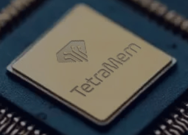
Why the 12 nm MLX300 matters for semiconductor design teams
Designers of edge AI silicon usually face a tradeoff between compute density and data movement. When model weights sit in external memory, a processor spends power and time shuttling operands across an interface. Analog in-memory computing attempts to reduce that movement by letting stored resistance states contribute to computation near, or inside, memory cells. Multi-level RRAM strengthens the concept because a single cell can represent more than two discrete levels, potentially increasing the information density available within the same array footprint.
The MLX300, however, should be evaluated with engineering caution. The public technical claims are focused on architecture, process migration, and model-scale support. A design team will still need to understand endurance, retention, write disturbance, analog nonlinearity, device-to-device variation, calibration, compiler mapping, and reliability qualification before concluding that a 12-nm A-IMC part can replace a conventional MCU-plus-NPU plus-DRAM chain in a commercial product.
Process migration: 22-nm, 2026, and the step to 12 nm
The earlier MLX200/MLX200M full-mask tapeout in 2026 was based on a commercial 22-nm process. That is an important baseline because it indicates the company had already moved beyond paper architecture into a manufacturable design submission using an established node. The new MLX300 tapeout shifts the same A-IMC and multi-level RRAM development direction into a 12-nm environment, which can imply smaller transistors, altered parasitics, different design-rule constraints, and a changed relationship between logic, memory array, and I/O.
For semiconductor observers, the word "tapeout" is not equivalent to high-volume production or customer-qualified supply. It marks the completion of a design ready for fabrication submission. The practical question is how many post-silicon bring-up cycles are needed, how the foundry and device stack mature, and whether the energy-efficiency and capacity claims remain after test.
EDA workflow: Synopsys and Synopsys Cloud FlexEDA
The MLX300 development used Synopsys EDA software delivered through Synopsys Cloud FlexEDA. This tooling detail matters because RRAM-based analog accelerators are not just digital netlists; the flow must handle mixed-signal behavior, memory-characterization models, design-for-manufacturing constraints, and verification across process corners. A cloud-delivered EDA access model also affects team scaling, license elasticity, and reproducibility of runs.
From a supply-chain and engineering-management view, the use of an established EDA vendor ecosystem suggests the chip program was built around mainstream commercial design infrastructure. The published article does not provide the specific tool set, calibration methodology, or foundry stack, so readers should avoid inferring PDK maturity or reliability from EDA access alone.
Architecture, capacity, and energy claims
MLX300 is presented as a single-chip accelerator aimed at audio, vision, and smaller language models. The stated capacity is support for up to 64 million INT4 parameters on-chip without external DRAM for model-weight storage. The stated energy-efficiency target is exceeding 50 TOPS/W.
These two numbers are useful because they connect directly to system architecture. INT4 quantization reduces the amount of data that must be represented for inference. If 64 million INT4 parameters can be held in memory-centric silicon, a product designer may question whether a separate LPDDR interface is needed for certain small-model workloads. Removing DRAM can shrink board area, lower component count, and reduce idle or interface power, but it also transfers weight-update, capacity, and yield considerations into the accelerator.
Comparison table: what the published article explicitly describes
| Design topic | Earlier RRAM A-IMC SoCs | MLX300 |
|---|---|---|
| Product family named | MLX200/MLX200M | MLX300 |
| Milestone context | Full-mask tapeout reported for 2026 | Tapeout completed; described as extending A-IMC development |
| Process node | 22-nm commercial process | 12 nm |
| Core memory technology | Multi-level RRAM | Multi-level RRAM |
| Compute concept | Analog in-memory computing SoC | Analog in-memory computing SoC |
| Stated model capacity | Not provided in the published article | Up to 64 million INT4 parameters on-chip |
| External DRAM for weights | Not provided in the published article | No external DRAM for model-weight storage is described for the stated capacity |
| Energy target | Not provided in the published article | Exceeding 50 TOPS/W |
| EDA path | Not provided in the published article | Synopsys tools via Synopsys Cloud FlexEDA |
Checklist: what to verify before treating the tapeout as a selection decision
- Confirm that the 12 nm node label corresponds to the production PDK intended for qualification, not only a research or multi-project design space.
- Ask how multi-level RRAM cells behave after repeated write cycles in the target inference workload.
- Request measured energy efficiency under the claimed 50 TOPS/W condition, not a simulated peak value.
- Clarify whether 64 million INT4 parameters are stored as native array states, mapped weights, or a system-level budget that still needs control logic.
- Review the impact of analog nonlinearity, noise margins, and process variation on model accuracy for audio, vision, and smaller language models.
- Check how Synopsys EDA flows through Synopsys Cloud FlexEDA support regression signoff, timing closure, and mixed-signal verification for the 12-nm implementation.
- Compare the MLX300 claim with the earlier MLX200/MLX200M 22-nm full-mask tapeout in 2026 to understand device-stack continuity.
Data citation and engineering interpretation
The published article supplies a compact set of quantitative anchors: a 12 nm MLX300 SoC, an earlier 2026 MLX200/MLX200M full-mask tapeout on a commercial 22-nm process, use of Synopsys EDA software through Synopsys Cloud FlexEDA, support for up to 64 million INT4 parameters without external DRAM for model-weight storage, and a target energy efficiency exceeding 50 TOPS/W. For an engineering audience, these are not just headline numbers; they are boundary conditions for evaluating whether the A-IMC path can change a bill of materials.
The value of this citation is that it separates process facts from inferred consequences. The article explicitly gives the node, product name, tooling route, parameter capacity, DRAM dependence, and efficiency target. It does not give post-silicon measurements, endurance curves, retention specifications, or production volume dates. Any stronger conclusion about a product must therefore come from additional characterization data, not from the tapeout announcement alone.
Common misconceptions
- A 12 nm tapeout automatically means the chip is production-ready. The milestone described is design completion for fabrication submission, not necessarily mass-production qualification.
- Analog in-memory computing removes all memory-system challenges. It may remove external DRAM for weights in the stated capacity case, but model mapping, update, retention, and accuracy still matter.
- Multi-level RRAM simply replaces a digital SRAM array with a smaller cell. Multi-level operation increases sensitivity to noise, variation, programming accuracy, and calibration.
- A higher 50 TOPS/W number proves a better product. Energy efficiency must be measured across model types, batch sizes, operating conditions, and end-to-end system power.
Action advice for engineers and procurement teams
- Hardware architects should first identify workloads that fit within 64 million INT4 parameters and can tolerate analog compute error budgets, especially always-on audio, constrained vision, and compact language-model inference.
- Design teams should build a risk register around endurance, retention, cell drift, programming time, and temperature behavior, then map those assumptions to product lifetime and field-service targets.
- Procurement analysts should distinguish a reported tapeout from qualified supply. Before including MLX300 in a product roadmap, request post-silicon data, production PDK status, and a clear migration path from MLX200/MLX200M.
- EDA managers should validate tool coverage for Synopsys Cloud FlexEDA usage, especially corner analysis, analog verification, and collaboration across geographically dispersed teams.
FAQ about the TetraMem RRAM A-IMC transition
What did TetraMem tape out?
The company reported completing the tapeout of MLX300, an A-IMC SoC built on multi-level RRAM technology and implemented at 12 nm.
How does this differ from the earlier MLX200/MLX200M work?
MLX200/MLX200M reached full-mask tapeout in 2026 on a commercial 22-nm process, while MLX300 extends the multi-level RRAM A-IMC direction into a 12-nm development environment.
Why is the Synopsys Cloud FlexEDA detail important?
Synopsys EDA software and cloud-delivered FlexEDA access indicate the program used mainstream commercial design infrastructure to carry a memory-centric analog architecture through SoC implementation.
What does 64 million INT4 parameters imply?
It suggests the stated architecture can hold a model-weight set of that size on-chip without external DRAM, potentially reducing interface-related cost and power for sufficiently small models.
Is exceeding 50 TOPS/W a guarantee?
The claim is described as a target, so it should be validated with measured, corner-case silicon performance rather than treated as a confirmed production specification.
Bottom line for Electronicseng readers
The MLX300 announcement is useful because it gives a concrete checkpoint in a memory-centric AI accelerator program: a 12 nm tapeout, a prior 22-nm reference point in 2026, an established EDA route through Synopsys Cloud FlexEDA, and explicit capacity and efficiency claims. For semiconductor engineers, the next step is not to celebrate node movement alone, but to trace each anchor back to measurement conditions. If the device stack can demonstrate stable multi-level RRAM behavior, repeatable programming, and system-level benefits without external DRAM, then the 12-nm step may matter beyond a roadmap update. If not, it remains a significant design milestone rather than a verified product transformation.