
Open-Loop LLC Control with Texas Instruments TPLD Logic: Electronicseng Semiconductors Guide
In isolated power stages where efficiency matters, LLC designs that do not need a closed control loop can move to simpler implementations. For Electronicseng readers evaluating semiconductor components and power-control architectures, the key question is not whether a dedicated closed-loop controller is available, but whether the system can accept a looser output tolerance while preserving required protection behavior. A closed-loop LLC controller can provide protection plus a precise ±3% regulated output, but an open-loop design may tolerate a ±10% unregulated output. In that case, many closed-loop functions are unnecessary and may need to be disabled.
Inductor-inductor-capacitor (LLC) converters commonly use a half bridge or full bridge on the primary side, selected according to voltage and power level. Synchronous rectification is often required for good efficiency, particularly at low output voltages. A programmable logic approach can shape the control signals, timing, soft start, enable behavior, and protection functions without always requiring a specialized controller for every block.
What a TPLD-based open-loop LLC controller must deliver
For semiconductor design teams, the practical starting point is to separate mandatory functions from optional functions. Mandatory functions include soft start, enable input, over-current protection (OCP) with cycle-by-cycle current limiting (hiccup mode or latch-off), and driving the primary-side power stage. Optional functions may include power-good output, over- and under-voltage lockout, and driving the synchronous rectifiers.
The Texas Instruments programmable logic device (TPLD) family can realize these features as a cost-effective open-loop solution. This does not mean that every LLC product should use a logic device; it means that when output regulation is relaxed to a ±10% unregulated output, the design may be simplified around the functions that are actually required.
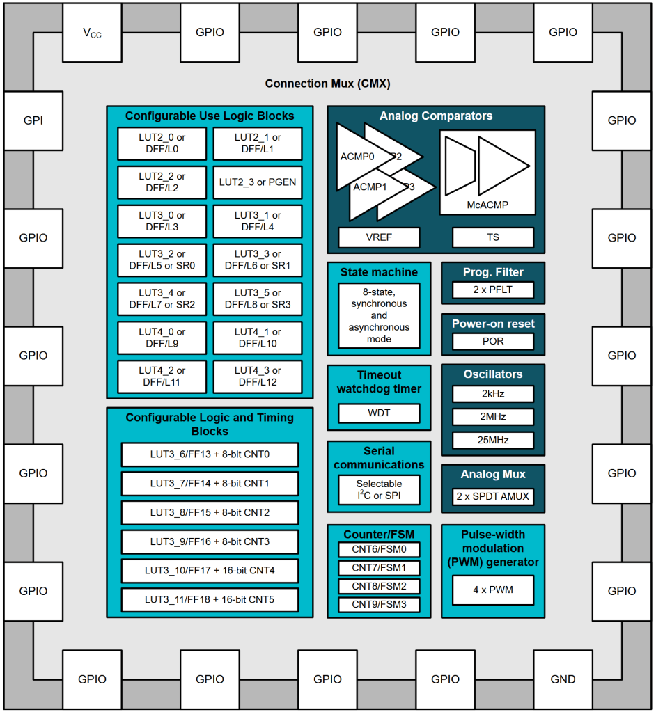
Figure 1: The TPLD2001-Q1 block diagram shows logic blocks, internal oscillators with a clock frequency up to 25MHz, a state machine, and analog comparators, matching the needs of an open-loop LLC controller. Source: Texas Instruments
Generating LLC and synchronous rectification timing with logic
Control-signal generation for the power stages is described as straightforward. At low switching frequencies, internal pulse-width modulation (PWM) generators may be used, while higher frequencies require a logic-based approach. One possible implementation is a classical ring buffer built from configurable one-shot blocks, which generate two inverted signals for the primary side and add dead time.
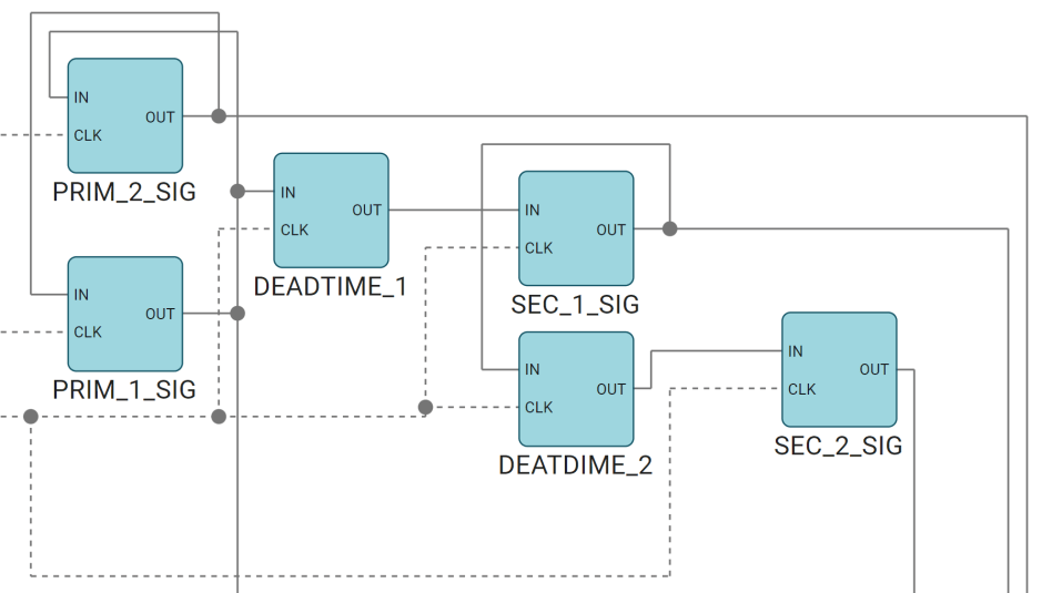
Figure 2: This example implementation generates two control signals for the primary side and two control signals for driving the synchronous rectifiers on the secondary side, with adjustable dead bands between primary and secondary, all within a single TPLD2001-Q1. Source: Texas Instruments
In this way, there is no need for a specialized synchronous rectifier controller. To enable synchronous rectification, a comparator channel can measure the primary-side current and enable synchronous rectification as soon as the converter input current rises above a decision threshold.
Figure 3 shows a design example using synchronous rectification without a specialized controller. The use of LMG2104-Q1 integrated half bridges simplifies the TPLD implementation, since these devices take care of the required dead time for the primary side by themselves.
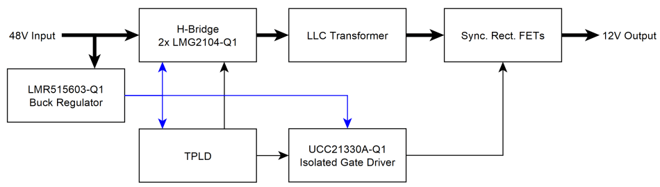
Figure 3: This overview of an example design uses the TI TPLD2001-Q1 as a controller. Source: Texas Instruments
Implementing OCP, soft start, and protection behavior
It is possible to achieve OCP using the internal comparators, which disable switching if the primary-side current gets too large. The amount of available logic gates enables an implementation that does cycle-by-cycle current limiting by skipping cycles if the primary-side current reaches a set limit.
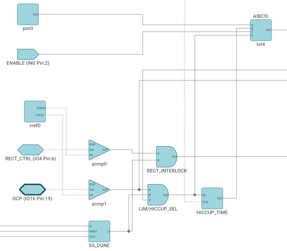
Figure 4: This example current-limit implementation also fits within the TPLD2001-Q1. Source: Texas Instruments
After a certain period of time, the control logic then enters hiccup mode or latch-off, which either one-shots or one of the TPLD counters can easily implement. Also, during soft start, the disabled synchronous rectification ensures that no unwanted current flows from the output back to the input of the converter.
An enable input completes the connectivity requirements and resets the device so that it goes through soft start when enabled. For devices with several analog inputs, it is easy to add under-voltage lockout and over-temperature protection features.
Frequency limits and timing constraints
There are limitations to these programmable logic devices, although many are easy to overcome. When using the internal PWM generators, the maximum frequency is limited to <100 kHz because of the fixed-period counter value. Because the open-loop LLC topology requires no duty cycle or frequency variation, designers can build their own control signal generator using the available logic cells within the TPLD2001-Q1 to achieve the desired output frequency.
A 25MHz clock frequency is high enough to generate suitable dead times and output signal frequencies up to about 500 kHz. Higher frequencies are possible; however, the dead time becomes an increasing percentage of the total switching cycle, thereby lowering efficiency. When using synchronous rectifier controllers and integrated power stages, which take care of the dead time by themselves, this efficiency penalty is no longer an issue.
| Timing or frequency item | Anchor from the reference design | Engineering interpretation |
|---|---|---|
| Internal PWM generator | <100 kHz | Useful when switching frequency stays within the fixed-counter limit. |
| Logic-based signal generator | about 500 kHz | Achievable by building the control-signal pattern from TPLD logic cells. |
| Clock resource | 25MHz | Provides resolution for dead time and output frequency generation. |
| Higher than 500 kHz | Higher frequencies are possible | Dead-time percentage rises, so efficiency may suffer unless the power stage handles timing itself. |
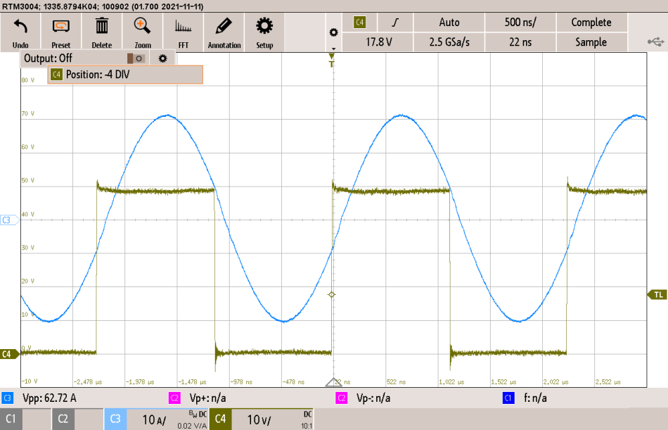
Figure 5: This graph from the design example shows the switch node and current waveform. Source: Texas Instruments
Selecting between TPLD2001-Q1 and TPLD1202-Q1
If no more than two analog inputs are needed, a smaller device such as the TPLD1202-Q1 is an option. But since that device has only one comparator, the inputs are multiplexed and therefore too slow for OCP. The discrete analog comparators available within the TPLD2001-Q1 are fast enough to implement OCP and can be used for other features like the previously described simple synchronous rectification control.
If OCP is the only analog feature that is required, the smaller TPLD1202-Q1 device variant may be a good fit for more cost-sensitive applications. For designs needing multiple analog functions, such as synchronous rectification detection plus OCP plus protection inputs, TPLD2001-Q1 is the more direct match in the referenced implementation.
| Device choice | Reference-design characteristic | Best use case |
|---|---|---|
| TPLD2001-Q1 | Includes discrete analog comparators and logic resources sufficient for the open-loop LLC example | Designs using OCP, synchronous rectification timing, soft start, enable, and other protection behavior in one logic device |
| TPLD1202-Q1 | Smaller device option; one comparator; inputs are multiplexed | More cost-sensitive cases where OCP is not required as an analog feature, or where fewer than three analog inputs are needed |
Design checklist for Electronicseng semiconductor readers
Use this checklist before deciding whether a TPLD-based open-loop solution fits the target converter:
- Confirm whether the application can accept a ±10% unregulated output instead of a precise ±3% regulated output.
- Identify which closed-loop functions can be removed or disabled, such as duty-cycle control or frequency modulation, if the open-loop topology requires no duty cycle or frequency variation.
- List mandatory functions: soft start, enable input, OCP with cycle-by-cycle current limiting, hiccup mode or latch-off behavior, and primary-side power stage driving.
- List optional functions: power-good output, over- and under-voltage lockout, and driving the synchronous rectifiers.
- Check the required switching frequency against <100 kHz for internal PWM, or determine whether a logic-based generator is needed for higher output signal frequencies.
- Verify that the 25MHz clock can produce acceptable dead times and output frequencies up to about 500 kHz without excessive dead-time percentage.
- Decide whether integrated power stages or synchronous rectifier controllers can absorb dead-time responsibility, reducing the efficiency penalty at higher switching frequencies.
- Count the analog inputs needed. If OCP must be fast, compare the TPLD2001-Q1 comparator path against the multiplexed single-comparator TPLD1202-Q1 path.
- Validate soft-start behavior so that disabled synchronous rectification prevents unwanted current from returning from output to converter input.
- Review system-level requirements such as bidirectional operation or higher switching frequencies, which could point to a different approach, including the Texas Instruments MSPM0 microcontroller.
Common misconceptions in open-loop LLC control
- Misconception: LLC control always needs a closed loop. Correction: Closed-loop LLC controllers are widely available and can provide precise ±3% regulated output, but open-loop cases may accept ±10% unregulated output, so some closed-loop functions are unnecessary.
- Misconception: The TPLD internal PWM generator can be used for every switching frequency. Correction: When using the internal PWM generators, the maximum frequency is limited to <100 kHz because of the fixed-period counter value.
- Misconception: 500 kHz is simply achieved by increasing clock speed without tradeoffs. Correction: Output signal frequencies up to about 500 kHz can be generated from logic cells using the 25MHz clock, but higher frequencies may make dead time an increasing percentage of the switching cycle, lowering efficiency.
- Misconception: TPLD1202-Q1 is always a low-cost drop-in. Correction: It has one comparator and multiplexed inputs, which are too slow for OCP, so it is more suitable when OCP is not the analog feature that must be implemented.
- Misconception: A logic device cannot replace specialized rectification control. Correction: In the referenced implementation, a comparator channel can measure primary-side current and enable synchronous rectification once converter input current rises above a decision threshold.
FAQ: open-loop LLC control with TPLD devices
Q: Why is open-loop LLC attractive for semiconductor power designs?
A: If the system can tolerate a ±10% unregulated output, the design may not need the precise ±3% regulation and associated closed-loop machinery. This can simplify the control function while still supporting soft start, enable behavior, OCP, and power-stage driving.
Q: What does TPLD contribute in the referenced architecture?
A: The Texas Instruments TPLD family can realize mandatory and optional functions in one programmable logic device. The TPLD2001-Q1 example includes logic blocks, internal oscillators up to 25MHz, a state machine, and analog comparators.
Q: How is dead time handled in the example?
A: One implementation uses configurable one-shot blocks in a ring buffer to generate two inverted primary-side signals and add dead time. When LMG2104-Q1 integrated half bridges are used, those devices handle the required dead time for the primary side themselves.
Q: When should a designer choose TPLD1202-Q1 instead of TPLD2001-Q1?
A: The smaller TPLD1202-Q1 is considered when no more than two analog inputs are needed. If OCP is the only analog feature required, it may be a fit for more cost-sensitive applications; however, its single multiplexed comparator path is too slow for OCP in the referenced comparison.
Q: When might the design need another approach?
A: If overall requirements include bidirectional operation or higher switching frequencies, device limitations could demand a different approach. In that case, the TI MSPM0 microcontroller could become a valid option.
Action recommendations for semiconductor and hardware teams
- Start from output tolerance, not controller complexity. Confirm whether the product specification accepts ±10% unregulated output before assuming a closed-loop LLC controller is required.
- Reduce the function list to the actual mandatory set. Keep soft start, enable, OCP, current limiting, hiccup or latch-off, and power-stage driving as core items, then review optional protection and status outputs separately.
- Use logic-based signal generation when internal PWM limits conflict with the switching target. The <100 kHz internal PWM boundary is useful at low frequency; the TPLD2001-Q1 logic approach supports output signal frequencies up to about 500 kHz with the 25MHz clock.
- Compare dead-time strategy before selecting the device. If integrated half bridges or synchronous rectifier controllers can manage dead time, the efficiency penalty at higher switching frequencies is reduced.
- Validate OCP timing early. Do not assume the smaller TPLD1202-Q1 can substitute for TPLD2001-Q1 when OCP needs a fast comparator path rather than a multiplexed single-comparator input.
- Escalate the architecture when requirements exceed open-loop assumptions. Bidirectional operation or higher switching frequencies may push the design toward a microcontroller approach such as MSPM0 instead of a purely logic-based controller.
Conclusion: where programmable logic fits in LLC design
The TPLD family offers enough flexibility to implement relatively complex control mechanisms for power converters. LLC applications that do not require a closed control loop can benefit from simple and low-cost implementation. The reference solution uses TPLD logic to generate control signals, synchronous rectification timing, soft start, enable behavior, and over-current protection within a device such as the TPLD2001-Q1. Although the example is based on a working solution, depending on overall requirements such as bidirectional operation or higher switching frequencies, some device limitations could demand a different approach. Here, the TI MSPM0 microcontroller could become a valid option.