
TSMC A14 Restarts 6T SRAM Scaling at 0.017 Square Micrometers: A Planning Guide for Semiconductor Teams
Cache area has behaved like a fixed tax on every new chip for the past several process generations, and that assumption is now the one worth re-examining. The A14 node from TSMC is expected to pull the 6T SRAM cell down to 0.017 square micrometers — the first genuine step backward in cell area since the 5 nm era opened. For semiconductor design, product planning and supply teams, the number matters less as a headline and more as a change to the inputs used in die-size, cost and roadmap calculations.
What has not moved since 2020
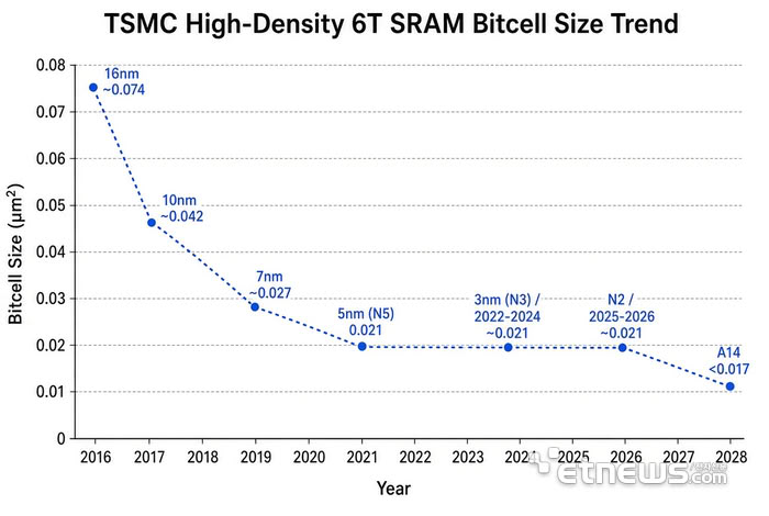
Progress on SRAM miniaturization at TSMC has been hard to detect for years. From the moment the N5 5 nm process entered mass production in 2020, the 6T memory cell held at roughly 0.021 square micrometers, generation after generation. Logic transistor density kept climbing across the same span, while the memory side never kept up. That split is why a cell-area figure now carries more planning weight than the nominal node name attached to it.

The A14 target: 0.017 square micrometers, about 19% smaller
The node expected to break that plateau is A14, planned for production in 2028. TSMC's 6T SRAM cell area is projected at 0.017 square micrometers, a reduction of about 19%. Getting there implies a specific technical breakthrough has been reached and is being prepared for large-scale volume production through A14 — not simply the incidental benefit of smaller logic transistors dragging memory along.
Key data referenced in this article, all of them vendor-stated figures for the A14 node rather than measurements from shipping silicon:
- 6T SRAM cell area held since the N5 5 nm process entered production in 2020: about 0.021 square micrometers
- 6T SRAM cell area projected on the A14 node in 2028: 0.017 square micrometers
- Cell-area reduction: about 19%
- SRAM density improvement relative to N2: 19%
- Logic density improvement relative to N2: 20%
- Speed uplift at equal power versus the N2 2 nm node: up to 15%
- Power reduction at equal frequency versus the N2 2 nm node: up to 30%
Where pilot production stands today
TSMC is currently running pilot production to assess the feasibility of the node and to let customers verify how their own designs behave inside a TSMC production environment. The development rhythm for A14 is described as optimistic, with early progress allowing part of the timetable to be pulled forward. If pilot work continues smoothly and no significant yield or manufacturing problems appear, risk production would start in 2027, followed by high-volume production in 2028. Should no obvious obstacles show up next year, TSMC may advance the mass production date by a few months.
A14 against the N2 2 nm node, parameter by parameter
| Parameter | N2 (2 nm node) | A14 | Planning implication |
|---|---|---|---|
| 6T SRAM cell area | Level held since N5 in 2020, about 0.021 square micrometers | 0.017 square micrometers | Cache-heavy blocks move off the flat line they have been on for years |
| SRAM density | Baseline reference | +19% | Direct benefit to designs where memory dominates area |
| Logic density | Baseline reference | +20% | Logic and memory shrink together, unlike recent generations |
| Speed at equal power | Baseline reference | Up to 15% faster | Headroom for performance targets without raising the power budget |
| Power at equal frequency | Baseline reference | Up to 30% lower | Thermal and battery-bound products gain margin at unchanged clock |
| Production status | Recently announced as in mass production | Pilot production; risk production in 2027; volume in 2028 | Only A14 is a future-window option for current programs |
| First fab site | Not stated in this brief | TSMC headquarters campus in Taiwan | Early capacity concentrates at one site |
Read as a whole, the comparison is the point that deserves attention: logic circuits and memory can now both achieve effective miniaturization across a meaningful generational gap, in sharp contrast with what happened during the sub-10 nm era. A14 will be introduced first at TSMC's headquarters campus in Taiwan, where the company plans to start production in 2028.
Common misreadings of the announcement
- Misconception: memory density has tracked logic density across recent nodes. Reality: the 6T cell sat at about 0.021 square micrometers from 2020 onward while logic transistor density kept rising.
- Misconception: the 15% and 30% figures can be stacked into one combined gain. Reality: they are two separate operating points — one measured at equal power, the other at equal frequency.
- Misconception: the SRAM improvement is a free by-product of logic scaling. Reality: SRAM density and logic density are reported as distinct improvements of 19% and 20% respectively, after years in which only logic moved.
- Misconception: 2028 is a locked date. Reality: risk production in 2027 is the gate, and a pull-in of a few months depends on no obvious obstacles appearing next year.
- Misconception: announcement means availability. Reality: the current pilot phase exists to evaluate feasibility and to let customers test their own designs inside TSMC's production environment.
Action checklist by role
Design and engineering teams
- Re-run cache and SRAM-heavy area estimates with a 0.017 square micrometer 6T cell instead of the 0.021 square micrometer figure that has been standard since 2020, and note where the ~19% cell-level gain does and does not translate into block-level area.
- Separate the two performance statements in your spec sheets: up to 15% speed at equal power is a different design trade-off from up to 30% power reduction at equal frequency.
- Where logic density (+20%) and SRAM density (+19%) both move, revisit partition decisions that were made when only the logic side was shrinking.
- Treat the pilot phase as a validation opportunity: the stated purpose includes letting customers check design behaviour inside a TSMC production environment.
Procurement and supply chain
- Build the risk production milestone in 2027 into supplier qualification and inventory models, ahead of the 2028 volume start.
- Plan for a possible pull-in of a few months if no obvious obstacles appear next year, rather than treating the published schedule as immovable.
- Note that the node will debut at TSMC's headquarters campus in Taiwan, and factor single-site concentration into early allocation risk.
Analysts and technology management
- Watch yield and manufacturing issues as the leading indicator: the schedule advance depends on pilot work staying smooth.
- Frame A14 as a memory-scaling event, not only a logic node step, since the break in a five-year plateau is the differentiating fact.
- Compare against the sub-10 nm era pattern when judging whether the density gains hold across subsequent generations.
FAQ
How long was the 6T SRAM cell stuck?
About five years of production history: from the time the N5 5 nm process entered mass production in 2020, the cell area remained roughly 0.021 square micrometers.
What does A14 actually change?
The 6T cell is projected to shrink to 0.017 square micrometers, a reduction of about 19%, with TSMC quoting a 19% SRAM density gain.
How does A14 compare with the N2 2 nm node?
Versus N2, A14 offers up to 15% higher speed at equal power or up to 30% lower power at equal frequency, plus a 20% logic density gain and a 19% SRAM density gain.
When will A14 be in volume production?
Risk production is planned for 2027 and high-volume production for 2028, provided pilot work continues without major yield or production problems. If no obvious obstacles emerge next year, the schedule could move earlier by a few months.
Where will it be manufactured first?
A14 will first be introduced at TSMC's headquarters campus in Taiwan, with production planned to start there in 2028.
Should current projects wait for A14?
Only where the roadmap bottleneck is on the memory side and the 2027 risk production to 2028 volume window fits the product launch; N2 is the option that is already declared in production.
The judgement to carry away
The significance of this node step is narrower and more useful than a density headline: after a stretch in which only logic shrank, both logic and memory are now expected to move across a real generational gap, with 6T SRAM down to 0.017 square micrometers. Until pilot production and the 2027 risk milestone clear, the right engineering posture is to treat the figures as targets, re-cost the designs that were sized around a stationary cache block, and keep the supply plan flexible enough to absorb a schedule that may still shift by a few months.